Boot Sequence: Case C
The following figure shows the interaction of the FPGA and SPI flash during booting.
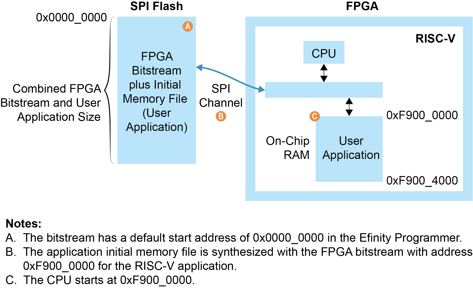
The boot sequence is:
- The system starts from the PC's 0xF900_0000, which is the starting address of the On-Chip RAM.
- The user application is already compiled with the bitstream. It starts executing automatically from the FPGA's BRAM.