PLL Auto Calibration and PLL Manual Calibration
| Block/Bus | Settings | |||||
|---|---|---|---|---|---|---|
| Mode | Register Option | Double Data I/O Option | Pull Option | Clock | Inverted Clock | |
| hbc_rst_n | output | register | – | – | – | – |
| hbc_cs_n | output | register | – | – | hbramClk | – |
| hbc_ck_p_HI | output | register | resync | – | hbramClk90 | Yes |
| hbc_ck_p_LO | output | register | resync | – | hbramClk90 | Yes |
| hbc_ck_n_HI | output | register | resync | – | hbramClk90 | Yes |
| hbc_ck_n_LO | output | register | resync | – | hbramClk90 | Yes |
| hbc_rwds_OUT_HI [1:0] | output | register | resync | – | hbramClk | Yes |
| hbc_rwds_OUT_LO [1:0] | output | register | resync | – | hbramClk | Yes |
| hbc_rwds_OE | output | register | – | – | hbramClk | – |
| hbc_rwds_IN_HI | input | register | resync | weak pulldown | hbramClk_Cal | Yes |
| hbc_rwds_IN_LO | input | register | resync | weak pulldown | hbramClk_Cal | Yes |
| hbc_dq_OUT_HI | output | register | resync | – | hbramClk | Yes |
| hbc_dq_OUT_LO | output | register | resync | – | hbramClk | Yes |
| hbc_dq_OE | output | register | – | – | hbramClk | – |
| hbc_dq_IN_HI | input | register | resync | weak pulldown | hbramClk_Cal | Yes |
| hbc_dq_IN_LO | input | register | resync | weak pulldown | hbramClk_Cal | Yes |
| Block/Bus | Settings | |||||
|---|---|---|---|---|---|---|
| Mode | Register Option | Double Data I/O Option | Pull Option | Clock | Inverted Clock | |
| hbc_rst_n | output | none | – | – | – | – |
| hbc_cs_n | output | register | – | – | hbramClk | – |
| hbc_ck_p_HI | output | register | normal | – | hbramClk90 | Yes |
| hbc_ck_p_LO | output | register | normal | – | hbramClk90 | Yes |
| hbc_ck_n_HI | output | register | normal | – | hbramClk90 | Yes |
| hbc_ck_n_LO | output | register | normal | – | hbramClk90 | Yes |
| hbc_rwds_OUT_HI [1:0] | output | register | normal | – | hbramClk | – |
| hbc_rwds_OUT_LO [1:0] | output | register | normal | – | hbramClk | – |
| hbc_rwds_OE [1:0] | output | register | – | – | hbramClk | – |
| hbc_rwds_IN_HI [1:0] | input | register | resync | weak pulldown | hbramClk_Cal | – |
| hbc_rwds_IN_LO [1:0] | input | register | resync | weak pulldown | hbramClk_Cal | – |
| hbc_dq_OUT_HI [15:0] | output | register | normal | – | hbramClk | Yes |
| hbc_dq_OUT_LO [15:0] | output | register | normal | – | hbramClk | Yes |
| hbc_dq_OE [15:0] | output | register | – | – | hbramClk | Yes |
| hbc_dq_IN_HI [15:0] | input | register | resync | weak pulldown | hbramClk_Cal | – |
| hbc_dq_IN_LO [15:0] | input | register | resync | weak pulldown | hbramClk_Cal | – |
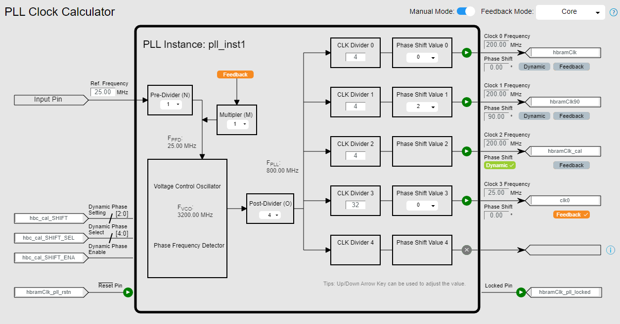
You must ensure that the dynamic phase shift has a 22.5 ~ 45 degree per step. The formula to calculate a single phase step coverage is given by:
Single phase step coverage = (0.5 x Post Divider (O) x Final Clock Out) / FVCO
x 360
Note: Efinix recommends that you set the
CLK Divider to 4 to get a 45° per phase shift for the
hbramClk, hbramClk90, and
hbramClk_cal clocks.| Target Clock Out Frequency | FVCO | Post-Divider (O) Setting |
|---|---|---|
| 250 | 4000 | 4 |
| 200 | 3200 | 4 |
| 150 | 4800 | 8 |
| 125 | 4000 | 8 |
| 100 | 3200 | 8 |
| 50 | 3200 | 16 |