AN 006: Configuring Trion FPGAs
About Configuring Trion FPGAs
This document describes how to configure Trion® FPGAs. These FPGAs contain volatile Configuration RAM (CRAM) that you must configure with the desired logic function (via a bitstream) upon power-up and before the core enters normal operation. The Efinity® software generates the bitstream, which is design dependent.
Bitstream Size
The bitstream size is dependent on the FPGA you choose and the configuration parameters you set in the Efinity software.
| FPGA | Maximum Supported Configuration Bits (Single Image) | Packages |
|---|---|---|
| T4 | 1,348,184 | All |
| T8 | 1,394,584 | BGA49, BGA81 |
| 5,255,968 | QFP144 | |
| T13 | 5,261,920 | All |
| T20 | 5,255,968 | QFP144 |
| 5,445,600 | WLCSP80, QFP100F3, BGA169, BGA256 | |
|
8,003,744
|
BGA324, BGA400 | |
| T35 | 8,139,168 | All |
| T55 | 27,675,040 | All |
| T85 | 28,042,400 | All |
| T120 | 28,409,760 | All |
Configuration Time
The FPGA configuration time depends on the frequency and data bus width. To estimate the configuration time for a given FPGA, use the following equation:
- T8 FPGA—approximately 1.38 Mbits of configuration data:
- Configuration clock frequency—10 MHz
- T8 Configuration data bus width—8 bits
Configuration time: 1.38 Mbits × 100 ns ÷ 8 = 17.25 ms
Planning Your Device Pinout
The configuration mode you choose affects your design's pinout. You should decide which mode you will use and plan for it before performing floorplanning or pin selection for your logic design.
Active and passive configuration modes use multi-function pins during configuration. When configuration completes, these multi-function pins are available for general use. JTAG configuration uses dedicated configuration pins that cannot be used for other functions. Additionally, the configuration mode you choose can affect the voltage restrictions for the I/O bank that contains the configuration pins.
Efinix® recommends that you:
- Choose the configuration mode(s). Consider the primary configuration mode as well as configuration modes you may need for debugging or future updates.
- Find the pin and the bank locations for the configuration mode(s).
- Understand how you use these pins and any restrictions when using multi-function
configuration pins as standard I/O pins. For example, consider internal and
external pull-ups or pull-downs, connections to external devices, etc. Note: In some situations, you may want to use a multi-function configuration pin as an output pin in user mode. If the pin is driven by an external device during configuration, the source that drives this pin during configuration must be tri-stated before the device enters user mode and user logic begins driving it. Otherwise, the drivers can be in contention, and can damage the pin.
- For each set of configuration pins, determine the common required I/O voltage support for the required configuration bank. You can only use compatible I/O standards elsewhere in that bank.
Other Factors to Consider
Although configuration is typically a one-time event independent of device operation, your configuration choices can affect your design options. Make configuration decisions early in the design cycle to eliminate challenges later:
- Do you need to support JTAG configuration for debugging purposes?
- How can you provide easy access to the configuration control and status pins for debugging?
- What multi-function pins are you using in your logic design and are they active during configuration? If they are, check for conflicts with other uses of these pins.
Additionally, you should:
- Provide quality signal integrity for key signals during PCB layout, including the configuration clock (even though configuration can operate at a low frequency).
- Understand the configuration sequence to reduce configuration time.
- Generate the configuration bitstream for your FPGA using Efinity tools.
Configuration Pins
- Dedicated pins cannot be used as general purpose I/O.
- During configuration, use dual-purpose pins as described in this document for the configuration mode you are using. After configuration (in user mode), you can use these pins as general-purpose I/O.
| Pins | Direction | Description | External Weak Pull- Up/Pull Down Requirement |
|---|---|---|---|
| CDONE | I/O | Configuration done status pin. CDONE is an open drain output; connect it to an external pull-up resistor to VCCIO. When CDONE = 1, the configuration is complete and the FPGA enters user mode. You can hold CDONE low and release it to synchronize the FPGAs entering user mode. | Pull up |
| CRESET_N | Input | Active-low FPGA reset and
re-configuration trigger. Pulse CRESET_N low for a duration of
tcreset_N before releasing CRESET_N from low to high
to initiate FPGA re-configuration. This pin does not perform a
system reset. |
Pull up |
| TCK | Input | JTAG test clock input (TCK). The rising edge loads signals applied at the TAP input pins (TMS and TDI). The falling edge clocks out signals through the TAP TDO pin. | Pull up |
| TMS | Input | JTAG test mode select input (TMS). The I/O sequence on this input controls the test logic operation . The signal value typically changes on the falling edge of TCK. TMS has an internal weak pull-up; when it is not driven by an external source, the test logic perceives a logic 1. | Pull up |
| TDI | Input | JTAG test data input (TDI). Data applied at this serial input is fed into the instruction register or into a test data register depending on the sequence previously applied at TMS. Typically, the signal applied at TDI changes state following the falling edge of TCK while the registers shift in the value received on the rising edge. Like TMS, TDI has an internal weak pull-up; when it is not driven from an external source, the test logic perceives a logic 1. | Pull up |
| TDO | Output | JTAG test data output (TDO). This serial output from the test logic is fed from the instruction register or a test data register depending on the sequence previously applied at TMS. The shift out content is based on the issued instruction. The signal driven through TDO changes state following the falling edge of TCK. When data is not being shifted through the device, TDO is set to an inactive drive state (e.g., high-impedance). | Pull up |
| Configuration Functions | Direction | Description | External Weak Pull- Up/Pull Down Requirement |
|---|---|---|---|
| CBUS[2:0] | Input | Configuration bus width select. CBUS has an internal weak pull-up. However, Efinix recommends that you use an external pull-up accordingly. See Selecting the Configuration Mode in AN 006: Configuring Trion FPGAs. | Pull up or pull down1 |
| CBSEL[1:0] | Input | Multi-image configuration selection pin. This function is not
applicable to single-image bitstream configuration or internal
reconfiguration (remote update). Connect CBSEL[1:0] to the external
resistors for the image you want to use: 00 for image
1 01 for image 2 10 for image 3 11
for image 4 0: Connect to an external weak pull
down. 1: Connect to an external weak pull
up. |
Pull up or pull down 2 |
| CCK | I/O |
Passive SPI input configuration clock or active
SPI output configuration clock (active low). Includes an internal
weak pull-up.
Important: The CCK pin in Q100F3
packages are only available in user mode when the LVDS TX
resources are not in use. The CCK pin should not be toggled when
any LVDS TX is used.
|
Optional pull up if required by external load |
| CDIn | I/O | n is a number from 0 to 31 depending on the SPI
configuration. 0: Passive serial data input or active serial
output. 1: Passive serial data output or active serial
input. n: Parallel I/O. In
multi-bit daisy chain connection, the CDI (31:0) connects to the
data bus in parallel. |
Optional pull up if required by external load |
| CSI | Input | Chip select. 0: The FPGA is not selected or enabled and will not
be configured. 1: Selects the FPGA for all configuration
modes. CSI must remain high throughout all configuration
modes. |
Pull up |
| CSO | Output | Chip select output. Selects the next device for cascading configuration. | N/A |
| NSTATUS | Output | Status (active low). Indicates a configuration
error. When the FPGA
drives this pin low, it indicates either a device mismatch or a
failed bitstream CRC check. For Trion® T4, T8 F49, and T8 F81 FPGAs, logic
low indicates a configuration error due to ID
mismatch. |
N/A |
| SS_N | I/O |
SPI configuration mode select. The FPGA senses the value of
SS_N when it comes out of reset (i.e., CRESET_N transitions from low
to high).
0: SPI Passive mode; connect to external weak pull down.
1: SPI Active mode; connect to external weak pull up.
In active configuration mode, SS_N is an active-low chip select to
the flash device (CDI0 - CDI3).
|
Pull up or pull down |
| TEST_N | Input | Active-low test mode enable signal. Set to 1 to disable test
mode. During all configuration modes, rely on the external weak
pull-up or drive this pin high. |
Pull up |
| RESERVED_OUT | Output | Reserved pin during user configuration. This pin drives high during
user configuration. F49 and F81 packages only. |
N/A |
| SPI_CS_N | Input | Active-low internal SPI flash memory chip select. Available in QFP100F3 packages only. | Pull up |
device_pinout.xlxs.FPGA Configuration Modes
Trion® FPGAs have dedicated configuration pins. You select the configuration mode by setting the appropriate condition on the input configuration pins. Trion® FPGAs support the following configuration modes.
| Mode | Description |
|---|---|
| SPI Active (serial/parallel) | The FPGA loads the bitstream itself from non-volatile SPI flash memory. |
| SPI Passive (serial/parallel) | An external microprocessor or microcontroller sends the bitstream to the FPGA using the SPI interface. |
| JTAG | A host computer sends instructions through a download cable to the FPGA's JTAG interface using JTAG instructions. |
Selecting the Configuration Mode
- Select the configuration mode by setting the appropriate condition on the
CBUS[2:0],SS_N, andTEST_Ninput pins. - Set
CBUS2,CBUS1,CBUS0,SS_N, andTEST_Nusing a pull-up or pull-down resistor, or drive them with an external active device. - Do not toggle the mode pins before the FPGA enters user mode.
| Configuration Mode | Parallel/Serial | CSI | TEST_N | SS_N | CBUS2, CBUS1, CBUS0 | Width |
|---|---|---|---|---|---|---|
| SPI Active | Serial | 1 | 1 | 1 | 3’b111 | x1 |
| Parallel | 1 | 1 | 1 | 3’b110 | x2 | |
| Parallel | 1 | 1 | 1 | 3’b101 | x4 | |
| SPI Passive | Serial | 1 | 1 | 0 | 3’b111 | x1 |
| Parallel | 1 | 1 | 0 | 3’b110 | x2 | |
| Parallel | 1 | 1 | 0 | 3’b101 | x4 | |
| Parallel | 1 | 1 | 0 | 3’b100 | x8 | |
| Parallel | 1 | 1 | 0 | 3’b011 | x16 | |
| Parallel | 1 | 1 | 0 | 3’b010 | x32 |
The JTAG/boundary-scan configuration interface is always available regardless of pin settings. If you send configuration instructions to the JTAG interface, the Trion® FPGA overwrites the previous configuration.
The supported configuration modes are FPGA specific. Refer to your FPGA's data sheet for information on the configuration modes it supports.
About SPI Clocking and Sampling
Serial Peripheral Interface (SPI) clocking and sampling determines how the FPGA and host exchange configuration data. Correct clock polarity, phase settings, and timing margins are essential to reliable configuration. The following table summarizes the passive vs active clocking behavior of Efinix Trion® devices.
| Mode | Clock | Sampling Edge |
|---|---|---|
| Passive | The CCK clock comes from an external device | Positive |
| Active | The FPGA generates the CCK clock | Positive (not configurable) |
The microprocessor or microcontroller can set the SPI clock polarity (CPOL bit) and the clock phase (CPHA bit) when the interface is idle, which results in four modes, depending on how you set these bits. Use Mode 3 in your microprocessor or microcontroller when programming the FPGA.
| Mode | Clock Polarity when Idle | Data Sampled On | Data Shifted On |
|---|---|---|---|
| 0 | Low | Rising edge | Falling edge |
| 1 | Low | Falling edge | Rising edge |
| 2 | High | Falling edge | Rising edge |
| 3 | High | Rising edge | Falling edge |
Efinix uses Mode 3 for SPI passive mode, which is CPOL bit = 1 and CPHA bit =1 for all Trion FPGA devices.

SPI Active Mode
In active mode, the FPGA loads configuration data itself
from a configuration bitstream that typically resides in non-volatile memory on the
same board. Active modes can be serial or parallel. The FPGA internally generates the
configuration clock signal (CCK) and controls configuration by
sending a clock or addresses to the flash memory.
The active SPI configuration mode supports low pin count, industry-standard external SPI flash devices to store the bitstream. The FPGA supports a direct connection to the flash device's four-pin SPI interface. Active SPI configuration mode can read from standard 1-bit serial SPI flash devices as well as from flash devices that support x2 and x4 fast output read operations. These modes are proportionally faster than the standard 1-bit SPI interface.
| Instruction | Description | SPI Data Width |
|---|---|---|
| 0BH | Fast Read | x1 |
| 3BH | Dual Output Fast Read | x2 |
| 6BH | Quad Output Fast Read | x4 |
The FPGA samples
CBUS0, CBUS1, and CBUS2 after
power-up or reconfiguration; therefore, you must drive these signals to the correct
value.3
Connection Examples
CRESET_N pin to meet the
tCRESET_N requirement.

CBUS values (see Table 5).CDI0 pin is a bidirectional data
I/O pin.
Timing
SS_N is a weak pullup. Then, the
FPGA: - Starts configuration by driving
SS_Nlow to wake up the external SPI flash. - Issues a release from power-down instruction to wake up the external SPI
flash by driving the
CDI0pin. - Waits for at least 30
µs. - Issues a fast read command to read the content of SPI flash from address 24h’000000. The maximum SPI flash address width for configuration is 24 bits.
- Optional: When configuration completes, the FPGA issues a deep power-down instruction to force the external SPI flash to enter into a deep power-down state.


SPI Active Mode for SIP Packages
Trion® FPGAs in QFP100F3 packages are a system-in-package (SIP) that includes an internal SPI flash that you can use to store configuration bitstreams. However, you can still use an external SPI flash to store the configuration bitstreams.
Depending on the setup, you must observe the following pin connection requirements in addition to the connections shown in Connection Examples.

Configuration with Internal Flash
For most use cases, Efinix recommends using the internal flash if you have only one or two configuration images. You can remove the external SPI flash connections if your user data is small enough that it can be stored in the internal SPI flash after storing the configuration images.
SS_NtoSPI_CS_NGPIOtoSPI Flash CS_B
- Configuration with internal SPI flash
- User data storage in external SPI flash

Configuration with External Flash
You will need to configure external flash if you have three or more configuration
images that exceeds the capacity of the internal SPI flash. You can remove the
connection between SPI_CS_N and GPIO if the
external SPI flash capacity is large enough for your application to free up the
GPIO.
SS_Nto SPI FlashCS_BGPIOtoSPI_CS_N
- Configuration with external SPI flash
- User data storage in internal SPI flash.

Additional Connection Requirements for SIP Packages
| Configuration Setup | SPI_CS_N Pin | External Flash Chip Select Pin |
|---|---|---|
| Configure with internal flash only | Connect to Trion® SS_N pin | Not applicable |
| Configure with internal flash | Connect to Trion® SS_N pin | Connect any Trion® GPIO pin |
| Configure with external flash | Connect any Trion® GPIO pin | Connect to Trion® SS_N pin |
SPI Active Mode without CSI
Trion®
FPGAs in smaller pin count packages,
such as the WLCSP80 and BGA169, may not have the
CSI signals bonded out. This pinout limits your programming
options. Without CSI, you cannot use cascade configuration.
CSI are the same as the regular SPI
active schematics except that you do not connect the CSI
signal.Clocking
An internal oscillator generates the internal clocks the FPGA uses during configuration. In SPI active configuration mode, configuration starts operating at the default frequency (10 MHz) and then switches to the user-selected clock to minimize configuration time (assuming the SPI flash device supports the faster fMAX).
You set the configuration clock frequency in the Efinity® software.
| SPI Clock Divider | Frequency (MHz) |
|---|---|
| DIV4 | 20 |
| DIV8 | 10 |
SPI Passive Mode
In passive mode, the FPGA receives the configuration clock and data from an external active module, such as an external microprocessor or microcontroller. This mode supports a data width of up to 32 bits.
Design considerations are similar to active configuration except CCK
must be driven from an external clock source. Each configuration image contains a
synchronization pattern. When the Trion®
FPGA detect the synchronization pattern, it begins
configuration. The external active device must supply data continuously on every
clock until configuration ends.
Connection Examples
These examples show SPI passive x1 and x32 modes. .

CS or CLOCK due to firmware
latency.CS of other devices sharing the
same SPI bus.You cannot disable the configuration by driving either SS_N to high or
CSI to low. You must complete the bit stream transmission before
communicating with other devices on the same SPI bus. The waveform as shown in Figure 11 results in successful configuration. While the waveform
as shown in Figure 12 results in configuration failure.


| CBUS | Byte Order | Bit Order |
|---|---|---|
| Cycle 1 | Byte 0 | Bit 7 (MSB) |
| Cycle 2 | Bit 6 | |
| Cycle 3 | Bit 5 | |
| Cycle 4 | Bit 4 | |
| Cycle 5 | Bit 3 | |
| Cycle 6 | Bit 2 | |
| Cycle 7 | Bit 1 | |
| Cycle 8 | Bit 0 (LSB) | |
| Cycle 9 | Byte 1 | Bit 7 (MSB) |
| Cycle 10 | Bit 7 | |
| Cycle 11 | Bit 5 | |
| Cycle 12 | Bit 4 | |
| Cycle 13 | Bit 3 | |
| Cycle 14 | Bit 2 | |
| Cycle 15 | Bit 1 | |
| Cycle 16 | Bit 0 (LSB) |

| CBUS | 31 | 24 | 23 | 16 | 15 | 8 | 7 | 0 | ||||||||||||||||
|---|---|---|---|---|---|---|---|---|---|---|---|---|---|---|---|---|---|---|---|---|---|---|---|---|
| Cycle 1 | Bit 7 (MSB) | Bit 0 (LSB) | Bit 7 (MSB) | Bit 0 (LSB) | Bit 7 (MSB) | Bit 0 (LSB) | Bit 7 (MSB) | Bit 0 (LSB) | ||||||||||||||||
| Byte 0 | Byte 1 | Byte 2 | Byte 3 | |||||||||||||||||||||
| Cycle 2 | Bit 7 (MSB) | Bit 0 (LSB) | Bit 7 (MSB) | Bit 0 (LSB) | Bit 7 (MSB) | Bit 0 (LSB) | Bit 7 (MSB) | Bit 0 (LSB) | ||||||||||||||||
| Byte 4 | Byte 5 | Byte 6 | Byte 7 | |||||||||||||||||||||
| CBUS | 15 | 8 | 7 | 0 | ||||
|---|---|---|---|---|---|---|---|---|
| Cycle 1 | Bit 7 (MSB) | Bit 0 (LSB) | Bit 7 (MSB) | Bit 0 (LSB) | ||||
| Byte 0 | Byte 1 | |||||||
| Cycle 2 | Bit 7 (MSB) | Bit 0 (LSB) | Bit 7 (MSB) | Bit 0 (LSB) | ||||
| Byte 2 | Byte 3 | |||||||
| Cycle 3 | Bit 7 (MSB) | Bit 0 (LSB) | Bit 7 (MSB) | Bit 0 (LSB) | ||||
| Byte 4 | Byte 5 | |||||||
| Cycle 4 | Bit 7 (MSB) | Bit 0 (LSB) | Bit 7 (MSB) | Bit 0 (LSB) | ||||
| Byte 6 | Byte 7 | |||||||
| CBUS | 7 | 0 | ||
|---|---|---|---|---|
| Cycle 1 | Bit 7 (MSB) | Bit 0 (LSB) | ||
| Byte 0 | ||||
| Cycle 2 | Bit 7 (MSB) | Bit 0 (LSB) | ||
| Byte 1 | ||||
| Cycle 3 | Bit 7 (MSB) | Bit 0 (LSB) | ||
| Byte 2 | ||||
| Cycle 4 | Bit 7 (MSB) | Bit 0 (LSB) | ||
| Byte 3 | ||||
| CBUS | Byte Order | 3 | 2 | 1 | 0 | ||||
|---|---|---|---|---|---|---|---|---|---|
| Cycle 1 | Byte 0 | Bit 7 (MSB) | Bit 6 | Bit 5 | Bit 4 | ||||
| Cycle 2 | Bit 3 | Bit 2 | Bit 1 | Bit 0 (LSB) | |||||
| Cycle 3 | Byte 1 | Bit 7 (MSB) | Bit 6 | Bit 5 | Bit 4 | ||||
| Cycle 4 | Bit 3 | Bit 2 | Bit 1 | Bit 0 (LSB) | |||||
| CBUS | Byte Order | 1 | 0 | ||
|---|---|---|---|---|---|
| Cycle 1 | Byte 0 | Bit 7 (MSB) | Bit 6 | ||
| Cycle 2 | Bit 5 | Bit 4 | |||
| Cycle 3 | Bit 3 | Bit 2 | |||
| Cycle 4 | Bit 1 | Bit 0 (LSB) | |||
| Cycle 5 | Byte 1 | Bit 7 (MSB) | Bit 6 | ||
| Cycle 6 | Bit 5 | Bit 4 | |||
| Cycle 7 | Bit 3 | Bit 2 | |||
| Cycle 8 | Bit 1 | Bit 0 (LSB) | |||
Timing
The microprocessor or microcontroller supplies the configuration clock and controls
the reset signal. The microprocessor or microcontroller must hold CRESET_N low for a duration of tCRESET_N and then release it to start the SPI
passive configuration. After tDMIN, the Trion®
FPGA samples the synchronization pattern and begins
configuration.


- Refer to Figure 11 for the supported waveform.
- The waveform shows the perspective from the control block without any optional external pull-up or pull-down resistors connected.
- CDI input data is clocked by
CCK. To prevent configuration failure,CCKmust stop toggling if the bitstream data becomes invalid. You must resume with the next bitstream data before stopping to continue the configuration. CSImust stay high during configuration.- It is recommended that
SS_Nremain low during configuration. Sometimes, however, an SPI Master might release theSS_Nto high during firmware latency. Refer to Figure 11 for the supported waveform. - Efinix does not recommend connecting multiple slaves on the same SPI bus to prevent signal contention.
- Refer to the data sheet for timing specifications.
SPI Passive Mode for SIP Packages
You can start SPI Passive configuration in QFP100F3 packages by pulling CDI3
low to prevent unexpected programming of the internal SPI Flash during SPI Passive configuration.

You need to drive CRESET_N low and CDI3 high with
the microprocessor if you intend to update the SPI flash data through the
microprocessor in user mode.
SPI Passive Mode without CSI or CBUS2
CSI or CBUS2
signals bonded out. This pinout limits your programming
options.- Without
CSI, you cannot use cascade configuration. - Without
CBUS2you can still useCBUS0andCBUS1to program using the passive serial x1, x2, and x4 modes.
The following figures show the schematics for programming without
CSI or CBUS2.


JTAG Mode
The JTAG serial configuration mode is popular for prototyping and board testing. The four-pin JTAG boundary-scan interface is commonly available on board testers and debugging hardware.
This section describes the JTAG configuration mode, for JTAG boundary-scan testing, refer to AN 021: Performing Boundary-Scan Testing on Trion FPGAs.
| Instruction | Binary Code [3:0] | Description |
|---|---|---|
| SAMPLE/PRELOAD | 0010 | Enables the boundary-scan SAMPLE/PRELOAD operation |
| EXTEST | 0000 | Enables the boundary-scan EXTEST operation |
| BYPASS | 1111 | Enables BYPASS |
| IDCODE | 0011 | Enables shifting out the IDCODE |
| PROGRAM | 0100 | JTAG configuration |
| ENTERUSER | 0111 | Changes the FPGA into user mode. |
| JTAG_USER1 | 1000 | Connects the JTAG User TAP 1. |
| JTAG_USER2 | 1001 | Connects the JTAG User TAP 2. |
| JTAG_USER3 | 1010 | Connects the JTAG User TAP 3. |
| JTAG_USER4 | 1011 | Connects the JTAG User TAP 4. |


The CRESET_N signal needs to be deasserted before
JTAG configuration begins. Only for T4, T8, T13, T20WLCSP80,
T20QFP100F3,T20QFP144, T20BGA256, and T20BGA169 FPGAs, drive
CRESET_N low, and then high prior to JTAG configuration.
When configuration ends, the JTAG host issues the ENTERUSER
instruction to the FPGA. After CDONE goes
high and the FPGA receives the ENTERUSER
instruction, the FPGA waits for tUSER to elapse,
and then it goes into user mode.


Design Considerations
- Because the
TCKandTMSsignals connect devices in the JTAG chain, they must have good signal quality. TCKshould transition monotonically at the receiving devices and should be terminated correctly. PoorTCKquality can limit the maximum frequency you can use for configuration.- Buffer
TMSandTCKso they have sufficient drive strength at all receiving devices. - Ensure that the logic high voltage is compatible with all devices in the JTAG chain.
- If your chain contains devices from different vendors, you might need to
drive optional JTAG signals, such as
TRSTand enables. - For Trion T4,
T8, T13, T20 (WLCSP80, QFP100F3, QFP144, BGA256, and BGA169 packages)
FPGAs:
- Drive
CRESET_Nlow and then high prior to JTAG configuration. - When using the Efinity programmer to perform
JTAG configuration, the
CRESET_NandSS_Npins are used in addition to the standard JTAG pins. If the JTAG-SPI bridge image has already been configured, neitherCRESET_NorSS_Nare required. However, you will need to establish bothCRESET_NandSS_Nconnections if using "Auto configure JTAG Bridge Image" in SPI flash programming through the JTAG bridge (see figure below).
- Drive
Using FPGA, MCU, and SPI Flash Devices Together
Most applications include some combination of FPGA, MCU, and SPI flash in the system design. How you connect the FPGA, MCU, and SPI flash determines the configuration mode and the configuration sequence.
MCU with Separate SPI Bus Connections
- FPGA images are stored in the SPI flash, allowing the MCU to configure the FPGA in SPI passive mode.
- In user mode, the MCU sends user data from the SPI flash to the FPGA.

FPGA with Separate SPI Bus Connections
SS_N, CCK,
CDI0, CDI1, CDI2, and
CDI3 pins are connected to the SPI flash; GPIO pins connect to the
MCU.- You use the SPI flash to store configuration images and application user data.
- In SPI active mode, the FPGA reads the configuration image from the SPI flash.

SS_N, CCK, CDI0,
CDI1, CDI2, and CDI3 pins are
connected to the MCU; GPIO pins connect to SPI flash.- Use SPI flash for storing application data.
- This system only supports SPI passive mode through the MCU.

Shared SPI Bus Connections
In the idle state, the SPI master disables the bus by setting the /CS
pin to high-impedance with an external pull-up, holding the signal high. In this
configuration, the flash and MCU share the FPGA’s SPI bus,
defaulting to SPI active mode after power up.
The state of the SS_N pin when CRESET_N is triggered determines the
configuration mode.


If you have an off-chip MCU, the configuration advice is the same as an006.html#concept_xxk_lwc_cdb__fig_arc_q3w_mqb with an SPI header.

Flash Programming Modes
The following table shows the methods you can use to program the configuration bitstream into the flash device on your board. Although you can program the flash directly using the SPI interface, this method requires that you have a SPI header on your board or use an FDTI chip. Therefore, Efinix recommends that you use a JTAG bridge, because that method only requires a JTAG header, which you would typically have on your board for other purposes.
| Mode | Description |
|---|---|
| SPI Active (serial/parallel) | Use the Efinity Programmer and a cable connected to a SPI header on the board. |
| SPI Active using JTAG Bridge (New) | A improved version of the SPI Active using JTAG Bridge (Legacy) mode with a faster flash programming time. |


| SRP1 | SRP2 | /WP | Status Register | Description |
|---|---|---|---|---|
| 0 | 0 | X | Software Protection | /WP pin has no control. Following a Write Enable instruction, the status register is writable, WEL=1. |
| 0 | 1 | 0 | Hardware Protected | When /WP is low, the status register is locked and is unwritable. |
| 0 | 1 | 1 | Hardware Unprotected | When /WP is high, the status register is unlocked. A Write Enable instruction will make the status register writable, WEL=1. |
| 1 | 0 | X | Power Supply Lock-Down | The status register is locked and cannot be written to again until the next power-up cycle. |
| 1 | 1 | X | One Time Program | The status register is permanently protected. |
Power Up
Power Up Sequence
Efinix® recommends the following power up sequence when powering Trion® FPGAs:


- Power up
VCCandVCCA_xxfirst. - When
VCCandVCCA_xxare stable, power up all VCCIO pins. There is no specific timing delay between the VCCIO pins. - For FPGAs with MIPI: Apply power to
VCC12A_MIPI_TX,VCC12A_MIPI_RX, andVCC25A_MIPIat least tMIPI_POWER afterVCCis stable.Important: Ensure the power ramp rate is within VCCIO/10 V/ms to 10 V/ms. - After all power supplies are stable, hold
CRESET_Nlow for a duration of tCRESET_N before assertingCRESET_Nfrom low to high to trigger active SPI programming (the FPGA loads the configuration data from an external flash device). - FPGA configuration can begin after there has been a tDMIN minimum
delay after
CRESET_Ngoes high (see SPI Passive and JTAG for the delay specification).
When you are not using the GPIO, MIPI, DDR or PLL resources, connect the pins as shown in the following table.
Power Supply Current Transient
You may observe an inrush current on the dedicated power rail during power-up. You must ensure that the power supplies selected in your board meets the current requirement during power-up and the estimated current during user mode. Use the Power Estimator to calculate the estimated current during user mode.
Power Up Configuration Circuitry Recommendation
You can use one of the following methods to hold the CRESET_N pin of the
Trion® FPGA low after the power supplies are stable:
- Supervisor integrated circuit (IC)
- Microprocessor or microcontroller
CRESET_N due to the improper power-up sequence.Supervisor IC Circuitry Example
Assuming that the VCCIO1A is the last power supply to be stable in the system, the
supervisor IC must hold the CRESET_N pin low for a duration of
tRP (reset timeout period) after the VCCIO1A reaches the stable
threshold.
Ensure that the tRP of the selected supervisor IC is more than the required tCRESET_N. Refer to the supervisor IC vendor for the recommended operating circuitry.

MR pin of the supervisor IC.Microprocessor or Microcontroller Circuitry Example

The microprocessor or microcontroller must hold the CRESET_N pin low
for longer than the required tCRESET_N duration.
Unused Resources and Features
| Unused Resource | Pin | Note |
|---|---|---|
| GPIO Bank | VCCIOxx | Connect to either 1.8 V, 2.5 V, or 3.3 V. |
| PLL | VCCA_PLL | Connect to VCC. |
| MIPI | VCC12A_MIPI_TX | Connect to VCC (1.2 V). |
| VCC12A_MIPI_RX | Connect to VCC (1.2 V). | |
| VCC25A_MIPI | Connect to VCC (1.2 V). | |
| DDR | VCCIO_DDR | Floating. Leave unconnected. |
| DDR_VREF | Connect to ground. |
Configuration Sequence
The Trion® FPGA configuration logic uses the following sequence during configuration:
- When
CRESET_Nreturns high (logic 1) after being held low (logic 0), the FPGA samples the logical value on itsSS_Npin. Like other programmable I/O pins, theSS_Npin has an internal pull-up resistor.Notice: Refer to the Trion® data sheet for the pulse width requirements ofCRESET_N. - If the
SS_Npin is sampled as a logic 1 (high), the FPGA configures using the SPI active configuration interface. - If the
SS_Npin is sampled as a logic 0 (low), the FPGA waits to be configured from an external controller or from another FPGA in SPI active configuration mode using an SPI-like interface.

Support for Multiple Images
When powered up in SPI active mode, the Trion® FPGA defaults to the first valid image it finds searching from address 0. If you enable the multi-image feature, you can optionally choose from three other images.
During multi-image configuration, the Trion®
FPGA monitors the CBSEL[1:0] pin logic
value when configuration or reconfiguration begins to determine which bitstream
image to use. Then, it loads the corresponding image starting from the address
specified in the bitstream option bits by sending out a fast read instruction
followed by the address.
For multi-image configuration, the Efinity® software saves the images to the bitstream file with no configuration bits between images by default.

24'h000000 address as Trion®
FPGAs always start searching for a valid bit stream from the
24'h000000 address.CBSEL[1:0] for the image you want to use:00for image 101for image 210for image 311for image 4
During configuration, the FPGA initially searches for a
valid image starting at the memory location 0x0000_0000 in the SPI
flash. It then proceeds to read the memory location based on the
CBSEL[1:0] setting. If no valid image is found at that memory
location, the FPGA continues to search in ascending
order until it locates a valid image. For example, if CBSEL[1:0] is
set to 11 and the SPI flash only contains valid images for
00 and 01, the FPGA will load the image from 00. The following table describes valid
and invalid images.
| Image Details | Note |
|---|---|
| Valid image | Configuration performs as expected. |
| Invalid image | FPGA The FPGA cannot recognize a valid image at the targeted SPI Flash address. It continues to search in ascending address and configure with the next valid image if any. |
| Corrupted image | Image is recognized, but the FPGA
fails in configuration with CDONE =
0 and NSTATUS = 0 to indicate
a device mismatch or CRC error (except T4, T8 F49,
and F81). |
CBSEL[1:0] pins. Refer to AN 010: Using the Internal Reconfiguration Feature to Update Efinix FPGAs Remotely for details on
this feature.Configuring Multiple FPGAs
- FPGAs that use the same configuration file can be loaded at the same time.
- FPGAs that use different configuration files (images) can be loaded sequentially, either through Trion® FPGAs in a daisy chain, or using external logic.
For daisy chain configurations, the Efinity® software includes 2,048 configuration bits between images in the bitstream file.
CSI signal bonded out (such as the WLCSP80 and
BGA169).Daisy Chaining with a SPI Flash Device
In a daisy chain, the FPGA closest to the configuration data source is the most upstream FPGA and the FPGA furthest from the source is the most downstream FPGA. The most upstream FPGA typically provides the configuration clock. All other FPGAs are in passive serial mode.
NSTATUS pins of multiple FPGAs together
when configuring in daisy chain configuration.

Daisy Chaining with a Microcontroller or Microprocessor
A microcontroller or microprocessor can configure FPGAs in a daisy chain with a single cascaded bitstream file. All FPGAs must be in passive mode.
This example shows serial daisy chain configuration with SPI passive x32
mode. For other modes, set the value of CBUS[2:0] according to Table 5.
NSTATUS pins of multiple FPGAs together
when configuring in daisy chain configuration.
Resistors in Configuration Circuitry
Alternatively, you can calculate your own pull-up or pull-down resistance, RUSER, shown in the following sections.
User-Defined Pull-Up Resistor Values
- RUSER = User-defined pull-up resistance
- RCPU = Combined pull-up resistance
- RIPU = Internal weak pull-up resistance
The combined pull-up resistance, RCPU, can be derived using the following formula:
- VT+ = Schmitt Trigger low-to-high threshold
- VCCIO = I/O bank power supply
- RIPD = Internal weak pull-down resistance
User-Defined Pull-Down Resistor Values
- RUSER = User-defined pull-down resistance
- RCPD = Combined pull-down resistance
- RIPD = Internal weak pull-down resistance
The combined pull-down resistance, RCPD, can be derived using the following formula:
- VT- = Schmitt Trigger high-to-low threshold
- VCCIO = I/O bank power supply
- RIPU = Internal weak pull-up resistance
Configuration Timing
Trion® FPGA configuration timing is process dependent. The following tables show the timing parameters for the various configuration modes.
| Symbol | Parameter |
|---|---|
| tCRESET_N | Minimum CRESET_N low pulse width required to trigger re-configuration. |
| tUSER | Minimum configuration duration after CDONE goes high before entering user mode. |
| Symbol | Parameter |
|---|---|
| fMAX_M | Active mode configuration clock frequency. |
| tSU | Setup time. |
| tH | Hold time. |
| Symbol | Parameter |
|---|---|
| fMAX_S | Passive mode configuration clock frequency. |
| tCLKH | Configuration clock pulse width high. |
| tCLKL | Configuration clock pulse width low. |
| tSU | Setup time. |
| tH | Hold time. |
| tDMIN | Minimum time between deassertion of CRESET_N to first valid configuration data. |
| Symbol | Parameter |
|---|---|
| fTCK | TCK frequency. |
| tTDISU | TDI setup time. |
| tTDIH | TDI hold time. |
| tTMSSU | TMS setup time. |
| tTMSH | TMS hold time. |
| tTCKTDO | TCK falling edge to TDO output. |
Flash Memory Support
SPI NOR flash is non-volatile memory accessed over the SPI bus that stores FPGA bitstreams and configuration data, enabling fast, deterministic reads so the Efinix FPGA boots reliably and supports safe in-field updates. Efinix has tested a number of third-party flash devices to determine their compatibility with Efinix FPGAs. The following sections provide an overview of tested flash devices, as well as the commands required to perform read and write actions on the flash memory.
Selecting the Right SPI NOR Flash Device
Trion® FPGAs support a SPI flash memory interface for active mode configuration. Use these guidelines to help choose the correct flash device for your Trion® FPGA.
- Configuration Bits—Ensure that your chosen flash device has enough bits
to store the configuration bitstream.
- Single image—Find the configuration bits a single image uses (refer to Table 1).
- Multiple images—Find the configuration bits a single image uses (refer to Table 1). Multiply the number of bits times the number of images to determine the total bits required to store the full bitstream.
- Daisy chain—Use the formula (i × b) + (2048 × (i - 1)) where i is the number of images and b is the configuration bits for each image. For example, a daisy chain of three T8 FPGAs uses (3 × 1,386,584) + (2,048 × (3-1)) = 4,159,752 + 4,096 = 4,163,848 bits.
- Configuration Bus Width—Determine the supported configuration bus width for the SPI flash device in Table 5.
- SPI Clock Frequency—Ensure that your SPI flash device supports a clock frequency that is higher than the SPI active configuration clock frequency as described in Table 10.
- Required Voltage—Make sure the voltage your SPI flash device requires is the same as the FPGA I/O bank voltage.
- Temperature Range—Check that the SPI flash device's temperature range is compatible with the operating temperature as described in the FPGA data sheet.
- Supported Instructions—Check that the SPI flash instruction set matches the M25-style of opcodes used by the Efinity Programmer and described in Table 27.
Verified SPI NOR Flash Devices
The following table lists third-party SPI flash devices tested and verified by Efinix as supported by Efinity Programmer.
| Manufacturer | Part Number | JEDED ID | Device ID (First Byte) |
Remark |
|---|---|---|---|---|
| Atmel (Adesto Technologies/Renesas/Microchip) | AT25DF6 | 0x1F | ||
| AT25SF | 0x84, 0x85, 0x86, 0x87, 0x88, 0x89, 0x8A | |||
| AT45 | 0x01 | |||
| EON | EN25Q | 0x1C | 0x30, 0x31, 0x38, 0x41, 0x42, 0x48, 0x60, 0x61, 0x70, 0x71, 0x73, 0x78, 0x7A | |
| Gigadevice | GD25LQ | 0xC8 | 0x60 | Does not support 4-byte address mode. |
| GD25WQ | 0x65 | |||
| GD25Q | 0x40 | |||
| ISSI | IS25WP | 0x9D | 0x70 | QE bit in Bit-6 Status Register-1 |
| IS25LP | 0x40, 0x60 | |||
| Macronix | MX25D6 | 0xC2 | 0x9E | QE bit in Bit-6 Status Register-1 |
| MX25E6 | 0x26 | |||
| MX25L | 0x20 | |||
| MX25U | 0x25, 0x95 | |||
| Micron | N25Q6 | 0x20 | 0xBA, 0xBB | |
| MT25Q | ||||
| Numonix | M25P6 | 0x20 | 0x71 | |
| M25PX6 | 0x20 | |||
| Puya | P25Q | 0x85 | 0x40, 0x42, 0x60 | |
| Spansion | S25FL | 0x01 | 0x02, 0x20, 0x60 | |
| SST (Microchip) | SST25 | 0xBF | 0x25 | |
| XTX | XT25F | 0x0B | 0x40 |
Supported Instructions
A SPI NOR Flash device is considered compatible if its instruction set implements the M25-style opcodes listed in Table 27, even when the device is not present in Table 26. If an unrecognized device is detected (i.e., JEDEC ID and device ID do not match), the Efinity Programmer will apply a generic flash profile for configuration images up to 2 GB.
| Instructions | Byte 1 | Byte 2 | Byte 3 | Byte 4 | Byte 5 | Byte 6 | Byte 7 | Byte 8 | Byte 9 |
|---|---|---|---|---|---|---|---|---|---|
| Read Device ID | 0xAB | Dummy | Dummy | Dummy | ID | N/A | N/A | N/A | N/A |
| Read JEDEC ID | 0X9F | Dummy | Dummy | Dummy | MF | N/A | N/A | N/A | N/A |
| Enable Reset | 0x66 | N/A | N/A | N/A | N/A | N/A | N/A | N/A | N/A |
| Reset Device | 0x99 | N/A | N/A | N/A | N/A | N/A | N/A | N/A | N/A |
| Write Enable | 0x06 | N/A | N/A | N/A | N/A | N/A | N/A | N/A | N/A |
| Read Status Register-1 | 0x05 | S[7:0] | N/A | N/A | N/A | N/A | N/A | N/A | N/A |
| Read Status Register-2 | 0x35 | S[15:8] | N/A | N/A | N/A | N/A | N/A | N/A | N/A |
| Write Register-1 | 0x01 | S[7:0] | N/A | N/A | N/A | N/A | N/A | N/A | N/A |
| Write Register-2 | 0x31 | S[15:8] | N/A | N/A | N/A | N/A | N/A | N/A | N/A |
| Read Data | 0x03 | A[23:16] | A[15:8] | A[7:0] | D[7:0] | D[7:0] | D[7:0] | D[7:0] | D[7:0] |
| Fast Read | 0x0B | A[23:16] | A[15:8] | A[7:0] | D[7:0] | D[7:0] | D[7:0] | D[7:0] | D[7:0] |
| Fast Read Dual Output | 0x3B | A[23:16] | A[15:8] | A[7:0] | Dummy | Dummy | D[7:0] | D[7:0] | D[7:0] |
| Fast Read Quad Output | 0x6B | A[23:16] | A[15:8] | A[7:0] | Dummy | Dummy | Dummy | Dummy | D[7:0] |
| 4 KB Sector Erase | 0x20 | A[23:16] | A[15:8] | A[7:0] | N/A | N/A | N/A | N/A | N/A |
| 32 KB Block Erase | 0x52 | A[23:16] | A[15:8] | A[7:0] | N/A | N/A | N/A | N/A | N/A |
| 64 KB Block Erase | 0xD8 | A[23:16] | A[15:8] | A[7:0] | N/A | N/A | N/A | N/A | N/A |
| Chip Erase | 0xC7 | N/A | N/A | N/A | N/A | N/A | N/A | N/A | N/A |
| Page Program | 0x02 | A[23:16] | A[15:8] | A[7:0] | D[7:0] | D[7:0] | D[7:0] | D[7:0] | D[7:0] |
Connecting Programming Hardware
You can program Efinix FPGA or the SPI flash using FTDI Mini Modules. This section describes the hardware connections required. See Using the Efinity Programmer for instructions about SPI and JTAG programming using the Efinity® Programmer.
Supported Download Hardware
| Manufacturer | Type | Part Number |
|---|---|---|
| FTDI | Dual Channel | FT2232 |
| Quad Channel | FT4232 | |
| Single Channel | FT232L | |
| Centron | Single Channel | Efinix Download Cable II |
SPI Programming Connections
The following figure illustrates the connection required when programming the SPI flash with FTDI FT2232H and FT4232H Mini-Module.


JTAG Programming Connections
Connecting a JTAG Cable
Efinix does not recommend using the FTDI cable C232HM-DDHSL-0 for JTAG programming due to the possibility of the FPGA not being recognized or the potential for programming failures.
Connecting a JTAG Mini-Module
When programming T4, T8, T13, T20WLCSP80, T20QFP100F3, T20QFP144, T20BGA256, and T20BGA169 FPGAs, use this connection:


CRESET_N and
SS_N pins in addition to the standard JTAG pins. However, this
setup is only needed for JTAG configuration. You can use the standard four JTAG pins
and any cable for other JTAG functions.When programming T20BGA324, T20BGA400, T35, T55, T85, and T120 FPGAs, use this connection:


Using the Efinity Programmer
The Efinity® software has a Programmer you use to configure Trion® FPGAs. You can run the Programmer using the GUI or with the command line.
Generate a Bitstream (Programming) File
When you run the automated flow, the software automatically generates bitstream files that you can use to configure your target device. You can also generate the bitstream files manually. To generate bitstream files from the command line, use the following command:
Generate a Bitstream File from the Command Line
> efx_run.py <project name>.xml --flow pgm> efx_run.bat <project name>.xml --flow pgm- .hex file as <project name>.hex. Use this file to program in SPI active or passive mode.
- .bit file as <project name>.bit. Use this file for JTAG programming.
The bitstream file includes programming options you set for your project (e.g., to initialize user memory or set configuration mode). If you change these options you must regenerate the bitstream file. See Project-Based Programming Options.
Working with Bitstreams
You can use the Efinity Programmer to manipulate a bitstream before programming an FPGA or flash device.
Edit the Bitstream Header
About this task
You can use the Programmer to edit the bitstream header information, for example, to add project or revision information. To edit the header:
Procedure
- In the Programmer, choose or click the toolbar icon to open the Edit Image Header dialog box. The window shows the default header information.
- Edit the header.
- Click Save.
Results
Device: <name>), the
Programmer may not be able to recognize the bitstream. Efinix
recommends that you only append a small amount of information to the auto-generated
data if you want to customize or annotate the header. The header can be a maximum of
256 characters, including the auto-generated text.Device: <name>
string.Export to Raw Binary Format
- Open the Programmer.
- Select the bitstream file.
- Click Export.
- Specify the filename.
- Click Save.
You can also convert the file to .bin at the command line as described in Convert to Intel Hex Format at the Command Line.
Export to .svf Format
- Open the Programmer.
- Select a bitstream file.
- Click Export.
- Specify the filename.
- Choose Serial Vector Format (*.svf) as the Files of type.
- Click Save.
Convert to Intel Hex Format at the Command Line
You can convert a bitstream file to Intel Hex and other formats at the command line using this command:
export_bitstream.py [--help] [--family FAMILY] [--idcode IDCODE] [--freq FREQ]
    [--sdr_size SDR_SIZE] [--tir_length TIR_LENGTH] [--hir_length HIR_LENGTH]
    [--tdr_length TDR_LENGTH] [--hdr_length HDR_LENGTH] [--enter_user_mode {on, off}]
format input_file output_file| Argument | Input | Description |
|---|---|---|
| format | hex_to_bin, hex_to_intelhex, bin_to_hex, intelhex_to_hex, hex_to_svf | Conversion type. |
| input_file | Filename | Image file source. |
| output_file | Filename | Image file destination. |
| Option (Long) | Option (Short) | Input | Description |
|---|---|---|---|
| --help | -h | None | Show help. |
| --family | N/A | Family name | Device family (SVF only) |
| --idcode | N/A | Identification code | JTAG IDCODE (SVF only). |
| --freq | N/A | Number | JTAG frequency (SVF only). |
| --sdr_size | N/A | Number | Approximate JTAG shift_dr size before cycling to
idle state (SVF only). |
| --tir_length | N/A | Number | JTAG bypass trailer instruction register length (SVF only). |
| --hir_length | N/A | Number | JTAG bypass header instruction register length (SVF only). |
| --tdr_length | N/A | Number | JTAG bypass header data register length (SVF only). |
| --enter_user_mode | N/A | on, off | Enter user mode after JTAG configuration (SVF only). |
The following example shows conversion of the bitstream hex file to bin format:
Converting Hex to Bin
%EFINITY_HOME%\bin\python3
%EFINITY_HOME%\pgm\bin\efx_pgm\export_bitstream.py hex_to_bin new_project.hex test2.bin
Combine Bitstreams and Other Files
You may want to store multiple bitstreams or other data into the same flash device on your board. For example, you can combine files for:
- Multi-image configuration using the
CBSELpins - Internal reconfiguration
- Programming FPGAs in a daisy chain
- Programming a bitstream and other files such as a RISC-V application binary
You use the Combine Multiple Image Files dialog box to choose files to combine into a single file for programming. Choose one of the following modes:
| Mode | Use For | Number of Images | Notes |
|---|---|---|---|
| Selectable Flash Image | Multi-image configuration | Up to 4 | Use this mode if you want the CBSEL pins to control which image the FPGA loads. For this mode, you also need to choose . See Program Multiple Images (CBSEL) |
| Internal reconfiguration | Up to 4 | Use this mode if you want the internal reconfiguration pins to determine which image the FPGA loads. For this mode, you also need to choose . See Program Multiple Images (Internal Reconfiguration) | |
| Daisy Chain | Daisy chains | Any number of JTAG devices including those from other vendors 7. | See Program a Daisy Chain |
| Generic Image Combination | A bitstream and other files | One bitstream and any number of other files | See Program Multiple Images (Bitstream and Data) |
SPI Programming
You can program Efinix FPGAs using the SPI interface and a .hex file.
Program a Single Image
About this task
In single image programming mode, you configure one FPGA with one image.
Procedure
- Click the Select Image File button.
- Browse to the outflow directory and choose <filename>.hex.
- Choose SPI Active or SPI Passive configuration mode.
- Click Start Program. The console displays programming messages.
Program Multiple Images (CBSEL)
About this task
In this programming mode, you specify up to four images that can configure one
FPGA. You then use the FPGA's CBSEL
pins to select which image to use. You can only use active
mode.
Procedure
- Click the Combine Multiple Images button.
- Choose .
- Enter the output file name.
- Choose the output file location. The default is the project's outflow directory.
- Choose . This setting tells the FPGA to use the CBSEL pins.
- Click in the table row corresponding to the position for which you want to add an image.
- Click Add Image.
- Select the image file to place in that location.
- Click OK.
- Repeat steps 6 through 9 as needed. You can add up to four images.
- Click Apply to generate the combined image file.
- Click Close to return to the Programmer, which displays the combined image file as the image to use for programming.
- Click Start Program.
Program Multiple Images (Internal Reconfiguration)
About this task
In this programming mode, you specify up to four images that can configure one FPGA. You then use the FPGA's internal reconfiguration interface to select which image to use. You can only use active mode.
Procedure
Results
Program Multiple Images (Bitstream and Data)
About this task
In this programming mode, you specify one bitstream and one or more data files to combine into a single file for programming. You can only use active mode.
Procedure
Results
Program a Daisy Chain
About this task
In this programming mode, you specify any number of images to configure a daisy chain of FPGAs. You can choose active or passive configuration for first FPGA; the rest are in passive mode.
Procedure
- Click the Combine Multiple Images button.
- Select Daisy Chain as the Mode.
- Enter the output file name.
- Choose the output file location. The default is the project's outflow directory.
- Click Add Image to add a file to the daisy chain.
- Repeat step 5 to add as many files as you want to the chain. Use the up/down arrows to re-order the images if needed.
- Click Apply to generate the combined image file.
- Click Close to return to the Programmer, which displays the combined image file as the image to use for programming.
- Click Start Program.
JTAG Programming
You can program Efinix FPGAs using the JTAG interface and a .bit file.
Trion Family JTAG Device IDs
The following table lists the Trion JTAG device IDs.
| FPGA | Package | JTAG Device ID |
|---|---|---|
| T4, T8 | BGA81 | 0x0 |
| T8 | QFP144 | 0x00210A79 |
| T13 | All | 0x00210A79 |
| T20 | WLCSP80, QFP100F3, QFP144, BGA169, BGA256 | 0x00210A79 |
| T20 | BGA324, BGA400 | 0x00240A79 |
| T35 | All | 0x00240A79 |
| T55, T85, T120 | All | 0x00220A79 |
Program a Single Image
About this task
In single image programming mode, you configure one FPGA with one image.
Procedure
- Click the Select Image File button.
- Browse to the outflow directory and choose <filename>.bit.
- Choose the JTAG configuration mode.
- Click Start Program. The console displays programming messages.
Program Using a JTAG Chain
About this task
You can program an FPGA that is part of a JTAG chain. The chain can include Trion® FPGAs as well as other devices. You define your JTAG chain using a JTAG chain file. You import the JTAG chain file into the Programmer to perform programming. The JTAG chain file is an XML file (.xml) that includes all of the devices in the chain. For example:
<?xml version="1.0"?>

<chain>
   <device chip_num="1" id_code="0x00210a79" ir_width="4" istr_code="1100" />
   <device chip_num="2" id_code="0x00210a79" ir_width="4" istr_code="1100" />
   <device chip_num="3" id_code="0x00210a79" ir_width="4" istr_code="1100" />
</chain>chip_numis the device order starting from position 1.id_codeis the hexadecimal JEDEC device ID (all lowercase letters)ir_widthis the width of the instruction register in bitsistr_codeis the binary IDCODE instruction
chip_num=”1” as the
first device.istr_code.To program using a JTAG chain:
Procedure
- Create a JTAG Chain File using a text editor.
- Open the Programmer.
- Choose your USB Target and Image.
- Select JTAG as the Programming Mode.
- Click the Import JCF toolbar button.
- Browse to your JTAG Chain File and click Open.
- Select which device you want to program in the drop-down list next to the JTAG Programming Mode option.
- Click Start Program.
Example
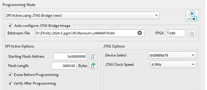
Program using a JTAG Bridge
About this task
Programming with a JTAG bridge is a two-step process: first you configure the FPGA to turn it into a flash programmer (.bit) and second you use the FPGA to program the flash device with the bitstream (.hex).
The SPI Active using JTAG Bridge mode (formerly named SPI Active using JTAG Bridge (New)) has pre-built flash loader (.bit) files that you can use. These .bit files do not require an external clock source. You can still use your own .bit file if you choose to do so.
To program using a JTAG bridge:
Procedure
- Choose the USB Target.
- In the Image box, click the Select Image File button to browse for the .hex file to program the flash device.
- Choose the SPI Active using JTAG Bridge programming mode.
- Turn on the Auto configure JTAG Bridge Image option.
-
Specify
your own
.bit file.
-
Choose the SPI Active Options and JTAG
Options.
Option Description Select Flash x8 mode only. Choose whether to use the upper flash, lower flash, or both. Starting Flash Address Specify the address if other than the default. Flash Length Specify the length if other than the default. Erase Before Programming Default: on. When turned on, the Programmer erases the flash device before re-programming it. Select Verify Method Normal verify—The FPGA computes an on-chip hash from the read back flash data to perform verification. Normal verify is significantly faster than in the Programmer v2024.2 and lower (so much faster that you might think it did not do anything). Fast verify—Similar to normal verify, but requires a SPI x4 width (quad mode). The Programmer cannot detect whether your board is using quad mode; if your board is not using it and you try to use fast verify, programming will fail.Skip verify—Do not verify the flash.Device Select Choose the JTAG device ID of the FPGA to program. JTAG Clock Speed Choose a speed or specify a custom one. - Click Start Program. The Programmer first configures the FPGA and then programs the flash device.
Results
JTAG Programming with FTDI Chip Hardware
About this task
These instructions describe how to program Trion® FPGAs using the FTDI Chip FT2232H and FT4232H Mini Modules. Efinix® has tested the hardware for use with Trion® FPGAs.
Procedure
- Open the Efinity® software.
- Open the Efinity® Programmer.
- Click the Select Bitstream Image button.
- Browse to your image and click OK.
-
Choose one of the following in the USB Target drop-down
list:
- Dual RS232 HS for FT2232H Mini Module
- FT4232H_MM for FT4232H Mini Module
- Choose JTAG from the Programming Mode drop-down list.
- Click Start Program.
FTDI Programming at the Command Line
The Efinity software includes a Python script you can use for programming FTDI modules at the command line.
ftdi_pgm.py [--help] [--mode MODE] [--output_file OUTPUT_FILE] [--url URL] [--aurl AURL]
    [--xml XML] [--num NUM] [--board_profile BOARD_PROFILE] [--address ADDRESS]
    [--num_bytes NUM_BYTES] [--burst_size BURST_SIZE] [--jtag_bridge_mode JTAG_BRIDGE_MODE]
    [--jtag_clock_freq JTAG_CLOCK_FREQ] [--verify_method VERIFY_METHOD]
    [--check_flash_if_supported CHECK_FLASH_IF_SUPPORTED] [--spi_active_freq SPI_ACTIVE_FREQ]
[--spi_passive_freq SPI_PASSIVE_FREQ] [--list_usb] [input_file]| Argument | Description |
|---|---|
| input_file | HEX file generated from efx_pgm. |
| Option (Long) | Option (Short) | Input | Description |
|---|---|---|---|
| --help | -h | None | Show help. |
| --mode | -m | passive, active, jtag, jtag_chain, erase_flash, read_flash, jtag_bridge, jtag_bridge_x8 | Programming mode. See the Efinity Programmer User Guide. In Efinity software versions prior to
v2025.1, the 8jtag_bridge and
jtag_bridge_new options were named
jtag_bridge_new and
jtag_bridge_x8_new, respectively.To use the JTAG
bridge modes, you must have already configured the with the JTAG SPI
flash loader. The Efinity software v2023.2
and higher includes pre-built flash loader.bit files in <
installation directory>/pgm/fli/<family>. Refer to
the JTAG SPI Flash
Loader Core User Guide for information on using the legacy
flash loader. |
| --output_file | -o | Filename | Output file used for read_flash mode. |
| --url | -u | URL | FTDI URL (see Identifying FTDI URLs). |
| --aurl | -a | URL | Alternative URL (Deprecated). |
| --xml | -x | Filename | XML file for JTAG programming. |
| --num | -n | Number | Chip target number for JTAG chain programming. |
| --board_profile | -b | Generic Board Profile Using FT232, Digilent JTAG-HS3, FireAnt Development Board, Generic Board Profile Using FT2232H, ISX Programming Cable, Titanium Ti180J484 Dev Board, Titanium Ti180M484 Development Kit, Generic Board Profile Using FT4232, JinChen Programming Cable, TJ180A484S Development Kit, Xyloni Development Board, Generic Board Profile Using FT4234HA | Name of the board profile used. |
| --address | N/A | Hex number | Starting flash address for flash read and write operations. |
| --num_bytes | N/A | Number | Number of bytes to erase or read. For modes erase
and read only. |
| --burst_size | N/A | Number | Individual read or write burst size in multiples of 256 bytes. For
legacy JTAG bridge modes only (jtag_bridge and
jtag_bridge_x8). |
| --jtag_bridge_mode | N/A | Erase, write, erase_and_write, read, all, all_no_erase | JTAG bridge programming mode. |
| --jtag_clock_freq | N/A | Number | JTAG clock frequency. |
| --verify_method | N/A | None, onchipx1, onchipx2, onchipx4 | The method used to verify the downloaded bitstream. Default:
onchipx2 (On-chip hash calculation with SPI x2 mode) |
| --check_flash_if_supported | N/A | Hex string | Check if flash is supported using the JEDEC ID hex string (e.g., C84012). |
| --spi_active_freq | N/A | Number | Set SPI active frequency. Default: 6000000 Hz |
| --spi_passive_freq | N/A | Number | Set SPI passive frequency. Default: 3000000 Hz |
| --list_usb | -l | None | List the available USB target's URL. |
Linux Examples
To program in Linux:
- Open a terminal and change to the Efinity® installation directory.
- Type:
source ./bin/setup.shand press enter. - Use the
ftdi_program.pycommand.
Example: Xyloni Development Board as the only board attached to your computer:
ftdi_program.py <filename>.bit -m jtagExample: Trion T120 BGA324 Development Board with serial number FT5ECP6E when another board with an FTDI chip is connected to your computer:
ftdi_program.py <filename>.bit -m jtag --url ftdi://ftdi:2232h:FT5ECP6E/1
    --aurl ftdi://ftdi:2232h:FT5ECP6E/1
Windows Examples
To program in Windows:
- Open a command prompt and change to the Efinity® installation directory.
- Type:
.\bin\setup.batand press enter. - Use the
ftdi_program.pycommand.
Example: Xyloni Development Board as the only board attached to your computer:
%EFINITY_HOME%\bin\python3
\ftdi_program.py <filename>.bit -m jtag
Example: Trion T120 BGA324 Development Board with serial number FT5ECP6E when another board with an FTDI chip is connected to your computer:
%EFINITY_HOME%\bin\python3
\ftdi_program.py <filename>.bit
    -m jtag --url ftdi://ftdi:2232h:FT5ECP6E/1 --aurl ftdi://ftdi:2232h:FT5ECP6E/1
Identifying FTDI URLs
Certain Efinity® scripts contain the --url and
--aurl options, which require the input of an FTDI URL.
--url and
--aurl options if you have more than one board with an FTDI chip
connected to your computer. The FTDI URL is in the format:
ftdi://ftdi:<product>:<serial>/<interface>where:
| <product> | Board |
|---|---|
| 232h | Trion T8 Development Board |
| 2232h | Trion T20 MIPI Development Board Trion T20 BGA256 Development
Board Trion T120 BGA324 Development Board Trion T120
BGA576 Development Board |
| 4232h | Xyloni Development Board |
- If you only have one Efinix® development board or FTDI device connected to your computer, you do not need to specify the serial number.
- In the Efinity® software v2020.2 and higher, the Programmer
displays the serial number of the FTDI device in the USB
Info string. The serial number is a string beginning with
FT.

<interface> is the interface number. For Efinix® development boards, <interface> is always 1.
Programmer Messages
The following section lists warning and error messages that the software may display and explains how to fix them.
| Message | on_program Device is not available |
| Reason | 1. Board not connected or powered off. 2. USB driver is not
installed. |
| To fix | 1. Connect board to host and power on the board. 2. Install USB
driver. |
| Message | USBError(2, 'Entity not found') |
| Reason | USB driver is not installed. |
| To fix | Install USB driver. |
| Message | *Cannot get JTAG url, Please check your board profile configuration*int() argument must be a string, a bytes-like object or a real number, not 'NoneType'--(idcode=None) |
| Reason | USB driver is not installed in interface 1 (JTAG). |
| To fix | Install USB driver for interface 1. |
| Message | ERROR: Incompatible file extension for programming mode, please use .bit file for JTAG programming |
| Reason | JTAG chosen as programming mode but .hex file specified in bitstream file. |
| To fix | Specify correct the .bit bitstream file. |
| Message | ERROR: Incompatible file extension for programming mode, please use .hex file for SPI Active programming |
| Reason | SPI Active chosen as programming mode but .bit file specified in bitstream file. |
| To fix | Specify correct the .hex bitstream file. |
| Message | ERROR: Incompatible file extension for programming mode, please use .hex file for SPI Passive programming |
| Reason | SPI Passive chosen as programming mode but .bit file specified in bitstream file. |
| To fix | Specify correct the .hex bitstream file. |
| Message | ERROR: Incompatible file extension for programming mode, please use .hex file for SPI Active using JTAG Bridge programming |
| Reason | SPI Active using JTAG Bridge chosen as programming mode but .bit file specified in bitstream file. |
| To fix | Specify correct the .hex bitstream file. |
| Message | ERROR: Incompatible file extension for programming mode, please use .hex file for SPI Active x8 using JTAG Bridge programming |
| Reason | SPI Active x8 using JTAG Bridge chosen as programming mode but .bit file specified in bitstream file. |
| To fix | Specify correct the .hex bitstream file. |
| Message | ERROR: Check board is plugged in, and then click on "Refresh USB Targets" |
| Reason | Board disconnected or powered off during programming. |
| To fix | Reconnect the board and click the refresh button. |
| Message | Image file not found |
| Reason | Bitstream file not loaded. |
| To fix | Load the bitstream file. |
| Message | Failure to configure was detected |
| Reason | Programmer internally failed to enter configuration mode. |
| To fix | Program again. |
| Message | Unable to configure from flash device. |
| Reason | JTAG state failed to enter USER mode. |
| To fix | Reprogram the bitstream. |
| Message | Unable to determine status of device. |
| Reason | 1. JTAG programming in unknown state; potentially hardware issue. 2. Different width
chosen to program the bitstream file. For example, the bitstream is x1
width but SPI Active x8 is chosen. |
| To fix | 1. Try to reprogram the bitstream. If using C323HM cable, check the
connectivity. 2. Choose the correct width or run the bitgen
again. |
| Message | ERROR: Flash verify unsuccessful... mismatch found |
| Reason | 1.Programmed flash does not match with the selected bitstream.2. The board does not support the selected verify method. |
| To fix | 1. Reprogram the bitstream.2. Select "Normal verify." |
| Message | ERROR: Unable to verify JTAG interface, cannot determine configuration status |
| Reason | JTAG mode used to program the board, but JTAG interface 1 is unstable or the JTAG connection using C2323HM is incorrect or disconnected. |
| To fix | Check the driver for the JTAG interface or check the wire connection. |
| Message | ERROR: Unknown error trying to read flash device, aborting. Aborting flash programmingFtdiProgram error: could not get flash device |
| Reason | Attempted to program the board via SPI Active or SPI Passive while interface 0 (SPI) is disabled. |
| To fix | Check the driver for the SPI interface. If it is unsupported (using C232HM), then it is not possible to program with SPI. |
| Message | FtdiProgram error: Device is in CONFIGURATION_FAIL state instead of user mode after programming JTAG Bridge Image! |
| Reason | Wrong or incomplete JTAG Bridge image specified. |
| To fix | Specify the correct JTAG Bridge image. |
| Message | Unsupported JTAG Bridge version: 0.0. Please choose the latest bundled JTAG Bridge image and then try again., aborting flash programming FtdiProgram error: |
| Reason | Used an older or unsupported version of the flash loader. |
| To fix | Use the supported version of the flash loader. |
| Message | ERROR: JTAG Bridge Image not found. Please specify correct file path.- ERROR: File = "" |
| Reason | JTAG Bridge image not specified when SPI Active using JTAG Bridge is selected as programming mode. |
| To fix | Specify the correct JTAG Bridge image. |
| Message | ERROR: Invalid speed entered, please only input numbers |
| Reason | Invalid character entered for Custom JTAG Clock Speed. |
| To fix | Use a numerical speed value. |
| Message | ERROR: Invalid speed entered, out of range, please enter a number between 1000 and 30,000,000" |
| Reason | Invalid character entered for Custom JTAG Clock Speed. |
| To fix | Use a valid value between 1000 and 30,000,000. |
| Message | ERROR: The FPGA given in the bitstream file does not match the FPGA you are trying to program. Check that you are using the correct bitstream file. |
| Reason | Wrong bitstream file specified for the board in use. |
| To fix | Specify the correct bitstream file. |
| Message | Detected 4Byte flag in bitstream but flash is smaller or equal to 16MiB Aborting flash programmingFtdiProgram error:Detected 4Byte flag in bitstream but flash is smaller or equal to 16MiB |
| Reason | 1. Erase or read flash attempted with a starting flash address greater than the flash
capacity. 2. Erase length specified greater than the flash
capacity. |
| To fix | 1. Specify the correct starting address. 2. Specify the correct length. |
| Message | ERROR: Unable to retrieve flash status Check board is plugged in, and then click on ""Refresh USB Targets"" Unrecognized Flash device. Will use Generic Flash profile. Please contact support if you face any problem. |
| Reason | Programmed bitstream contains an incorrect or mismatched header with the board. |
| To fix | Verify that the bitstream header is correct. |
| Message | ERROR: Export SVF feature is disabled for T8/T20 bitstreams |
| Reason | T8 or T20 bitstream exported to SVF. |
| To fix | SVF is not supported for T8 or T20. |
| Message | ERROR: Cannot edit SPI Active clock settings for .bit file, please use the .hex file |
| Reason | Opened Edit SPI Active Clock on a .bit file. |
| To fix | Edit SPI Active Clock only works for .hex files. |
| Message | ERROR: Input file has been corrupted, unable to determine target device |
| Reason | Opened Edit SPI Active Clock on a corrupted .hex file. |
| To fix | Replace the corrupted .hex file to a valid one. |
| Message | ERROR: Unable to read input image file, file maybe have been corrupted |
| Reason | Opened Edit SPI Active Clock on a corrupted .hex file. |
| To fix | Replace the corrupted .hex file to a valid one. |
| Message | ERROR: Device code for JTAG Bridge image CANNOT be Unknown. Please ensure you are using correct bitstream file |
| Reason | 1. Programmer is unable to detect the device code. 2. Connectivity issue. 3. USB
driver missing for the JTAG interface. 4. Programmer is unable to
detect non-Efinix device. |
| To fix | Ensure there is a valid device ID at Device Select. |
| Message | ERROR: Export feature only works with Efinity bitstreams |
| Reason | Export failed because the bitstream is not originally from Efinity. |
| To fix | Bitstream exports not originally from Efinity are not supported. |
| Message | ERROR: Cannot detect JTAG chain setup. Please import JTAG chain file |
| Reason | Programmer is unable to detect non-Efinix device. |
| To fix | Import the JCF. |
| Message | Calculated IR width is invalid. Please import JTAG chain file |
| Reason | A board in the chain is powered off. |
| To fix | Power on the board and click the refresh button. |
| Message | Total IR width of the previous JCF does not match actual total IR width. Please import JTAG chain file again. |
| Reason | Programmer is unable to detect non-Efinix device and cannot auto-detect IR length of the board in the JTAG chain. |
| To fix | Import the JCF. |
| Message | ERROR: The Programmer cannot detect the FPGA in the JTAG chain. Check the JTAG cable or header for connectivity issues |
| Reason | Incorrect connection of the chain or improperly connected wire. |
| To fix | Check the wire connectivity and check the IDCODE through the SVF Player. |
| Message | ERROR: Invalid ASCII character detected in header, cannot display header text |
| Reason | Bitstream header is incorrectly formatted. |
| To fix | Run the bitstream again to generate a new bitstream. |
| Message | ERROR: JTAG chain file does not match XSD standard |
| Reason | The JCF file in the wrong format. |
| To fix | Fix the format of the JCF. |
| Message | Error occurred. OpenocdNotRunning("An error occurred when waiting for response from the main loop. OpenocdNotRunning('Failed to add a user due to: OpenOCD Error: no device found; Return code: 1')") |
| Reason | Occurs in co-debug mode when the board is disconnected and reconnected. |
| To fix | Close and re-open the Programmer. |
| Message | Failed to detect number of JTAG TAP. JTAG chain connection may be broken or number of TAP is greater than 128 |
| Reason | Failed to auto-detect the board in the JTAG chain. |
| To fix | Import the JCF. |
| Message | ERROR: Invalid output file <file name> specified for image generation |
| Reason | Name of the output file not specified when using Combine Multiple Image Files. |
| To fix | Specify the file in Output File. |
| Message | ['', '', '', '']ERROR: All input files for image generation must be targeted to the same device |
| Reason | 1. No file added to the field at Combine Multiple Image Files. 2. Image mixed with a
different target device. |
| To fix | 1. Add at least one image to use the tool. 2. Only the same targeted device bitstream file
can be used to combine the image. |
| Message | ERROR: Flash address '' is not a valid hexadecimal number |
| Reason | Flash address unspecified or incorrect at Generic Image Combination. |
| To fix | Specify the flash address in the correct hexadecimal format. |
| Message | ERROR: No input files for image combination |
| Reason | No input file specified for the image combination at Generic Image Combination. |
| To fix | Specify at least one image. |
| Message | ERROR: First flash address '0x00380000' is not equal to 0x00000000 |
| Reason | First flash address specified at Generic Image Combination does not start with 0. |
| To fix | For the first image, the flash address must start with 0. |
| Message | ERROR: Flash address '0x00000000' should be greater than or equal to next availableflash address '0x00121000' |
| Reason | Second or later flash address specified at Generic Image Combination starts with 0. |
| To fix | For the second and later images, the flash address cannot start with 0. |
Using the Command-Line Programmer
To run the Programmer using the command line, use the command:
Command-Line Programmer
efx_run.py <project name>.xml --flow program [--pgm_opts [mode=MODE] [settings_file]]efx_run.bat <project name>.xml --flow program [--pgm_opts [mode=MODE] [settings_file]]Options
--pgm_opts mode specifies the configuration mode. The available modes
are:
| Mode | Description |
|---|---|
| active | SPI Active configuration. |
| passive | SPI Passive configuration. |
| jtag | JTAG programming. See the Efinity Programmer User Guide for more information about programming with the JTAG interface. |
| jtag_bridge | SPI Active using JTAG bridge mode. |
| jtag-bridge_x8 | SPI Active x8 using JTAG bridge mode (used with two flash devices). 9 |
efx_run.py <project name>.xml --flow program --pgm_opts mode=jtag--pgm_opts
settings_file specifies a file in which you have saved all of the
programming options. A settings file is useful for performing batch programming of
multiple devices.
Project-Based Programming Options
You specify project-based programming options in the tab in the Efinity® software. Efinix FPGAs support active and passive configuration in a variety of modes.
| Option | Notes |
|---|---|
| Active/Passive | Active: SPI active mode. Passive: SPI passive mode. Your
choice of active or passive affects the pinout and determines which
choices are available in the Programming Mode box. |
| JTAG USERCODE | Fixed
at: 0xFFFFFFFF |
| Clock Source | For Trion
FPGAs, this option is always
Internal Oscillator. |
| SPI Programming Clock Divider | Choose the divider for the SPI clock. This setting is reflected in
the bitstream file. Default: DIV8 |
| Clock Sampling Edge | For Trion
FPGAs, this option is
always Rising. |
| Power down flash after programming | Enable this option to power down the flash device after the FPGA finishes programming.
This setting is reflected in the bitstream file, and you can only set it
here. Default: On |
| Use 4-byte addressing during configuration | This
option is not supported for all Trion
FPGAs. |
| Programming mode | Choose the programming mode and width; the choices depend on the FPGA and package you are
targeting. This setting is reflected in the bitstream file, and you can
only set it here. Default: SPI <active or passive>
x1 |
| Enable Initialized Memory in User RAMs | This setting is reflected in the bitstream file, and you can only set
it here. on: The bitstream has initialized
memory. off: The bitstream does not
have initialized memory. smart: For the Trion family,
this option has the same effect as
on. |
| Release Tri-States before Reset | During configuration, core signals are held in reset and the I/O pins
are tri-stated. These states are released when the FPGA enters user
mode. On: (default) I/O pins are released from tri-state before
the core is released from reset (use this option when the
application is core sensitive). Off: Core signals are
released from reset before the I/O pins are released from tri-state
(use this option when the application is I/O
sensitive). |
| Generate JTAG configuration file | On (always): Generate a .bit file for JTAG configuration. |
| Generate JTAG raw binary configuration file | On: Generate a .bin file (raw binary) for JTAG
configuration. Off (default): Do not generate a
.bin file. |
| Generate SPI configuration file | On (always): Generate a .hex file for SPI programming. |
| Generate SPI raw binary configuration file | On: Generate a .bin file (raw binary) for SPI
programming. Off (default): Do not generate a
.bin file. |
When you change one of these options, you can simply re-run the bitstream generation flow step. You do not need to recompile the design.
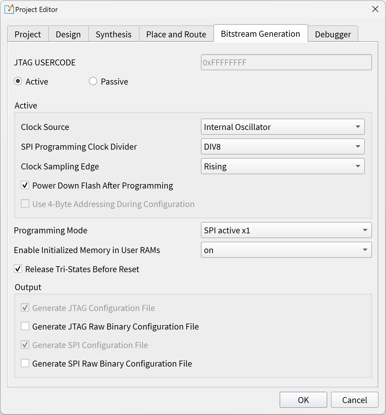
Verifying Configuration
You can confirm that the FPGA is configured by your bitstream successfully by checking on the following:
- Use the Efinity Programmer to check whether the FPGA is in user mode. In the Programmer, click the button. The console displays the FPGA status.
- Monitor the
CDONEandNSTATUSpins to determine the status of the FPGA. The status lets you know if there is a configuration error (CDONE=0andNSTATUS=0). - You can verify the bit stream stored in the SPI flash after programming is
completed in SPI Active mode. Turn on the option in to check for errors such as flash image being corrupted
during a write, an improperly skipped erase step, etc.Note: Generally, Efinix recommends that you keep the Verify After Programming option turned on. However, if you are using the FPGA's built-in CRC checking (enabled by default) with
NSTATUSmonitoring to verify configuration, you can use that method as a way of verifying the flash (that is, if the FPGA goes into user mode, the flash write is verified).Note: The Verify After Programming confirms the correctness of the bitstream programmed into the SPI Flash. It does not confirm if the device is in use afterwards.
CDONE = 0 and NSTATUS =
0. The CRC check can be useful for debugging board problems
such as signal integrity issues between the flash device and the FPGA. In some cases, you may need to debug possible configuration errors. To simplify this debugging process, add logic to your RTL design that generates a signal you can monitor to confirm that the FPGA has entered user mode.
Monitoring with the Efinity Programmer
With the board connected to your computer, you can monitor the FPGA's status with the Programmer. The
following table describes the values of CDONE and
NSTATUS and their meaning.
| CDONE | NSTATUS | Programmer Message | Description |
|---|---|---|---|
| 0 | 0 | Failure to configure was detected | Configuration failed. This may be cause by:
|
| 0 | 1 | Programming ... | The FPGA is in configuration mode. |
| 1 | 0 | – | The FPGA is in transition from configuration mode to user mode conditionally. |
| 1 | 1 | Device is in user mode! | The FPGA is functioning correctly according to the user design. |
NSTATUS is a dual purpose GPIO, you may
observe different behavior from Efinity
Programmer on NSTATUS if NSTATUS is applied as a
GPIO in your bit stream.Monitoring with a Microcontroller or LEDs
You can optionally monitor the status of CRESET_N,
CDONE and NSTATUS with a microcontroller or
LEDs. CDONE is a dedicated configuration pin and you can monitor it
directly. However, NSTATUS is a dual-purpose configuration pin. To
use it to monitor configuration, you can connect it to a GPIO and set its output
value to a constant 0.
NSTATUS to your design as a GPIO for monitoring: - In the Interface Designer, create a GPIO block for
NSTATUSwith the following settings:- Instance Name: NSTATUS
- Mode: Output
- In the Instance View pane, assign the
NSTATUSinstance to theNSTATUSpackage pin (refer to the pinout file to find the package pin). - Follow these steps to set the external or internal configuration:
- For single image (SPI active, SPI passive, and JTAG) and external
controller flash image,
- Set Constant Output:
0 for the
NSTATUS
- Set Constant Output:
0 for the
- For internal configuration,
- Assign the
cfg_errorto theNSTATUSin the RTL top module.
- Assign the
- For single image (SPI active, SPI passive, and JTAG) and external
controller flash image,
- Recompile the design.
- Download the bitstream to the flash memory on your board.
CDONE and
NSTATUS pins:
- Reset the FPGA.
- Poll
CDONEfor1. - Wait for
tUSER. - Sample
NSTATUS.
| CRESET_N | CDONE | NSTATUS (After tUSER) | Description |
|---|---|---|---|
| 1 | 0 | 0 | Configuration failed. This may be caused by:
|
| 1 | 0 | 1 | The FPGA is in configuration mode. |
| 1 | 1 | 0 | The FPGA is functioning correctly according to the user design. |
| 1 | 1 | 1 | For internal reconfiguration only. The targeted application image FPGA cannot be configured successfully after six trials or a timeout with the golden image restored. |
The following figure shows example schematics connecting LEDs to the FPGA's CDONE and
NSTATUS pins:

| CRESET_N | CDONE LED | NSTATUS LED | Description |
|---|---|---|---|
| 1 | Off | Off | The FPGA is in configuration mode. |
| 1 | Off | On | Configuration fails. This may be caused by:
|
| 1 | On | On | The FPGA is functioning correctly according to the user design. |
| 1 | On | Off | The internal reconfiguration only, the targeted application image cannot be configured successfully after 6 trials or a timeout with the golden image restored. |
Installing USB Drivers
To program Trion® FPGAs using the Efinity® software and programming cables, you need to install drivers.
Efinix development boards have FTDI chips (FT232H, FT2232H, or FT4232H) to communicate with the USB port and other interfaces such as SPI, JTAG, or UART. Refer to the Efinix development kit user guide for details on installing drivers for the development board.
For your own development board, Efinix suggests using the FTDI Chip FT2232H or FT4232H Mini Modules for JTAG programming Trion® FPGAs. (You can use any JTAG cable for JTAG functions other than programming.)
| Board | Connect to Computer with |
|---|---|
| Efinix development boards | USB cable |
| Your own board | FTDI x232H programming kit. For example:
|
Installing the Linux USB Driver
The following instructions explain how to install a USB driver for Linux operating systems.
- Disconnect your board from your computer.
- In a terminal, use these
commands:
> sudo <installation directory>/bin/install_usb_driver.sh
> sudo udevadm control --reload-rules
> sudo udevadm trigger
Installing the Windows USB Driver
On Windows, you use software from Zadig to install drivers. Download the Zadig software (version 2.7 or later) from zadig.akeo.ie. (You do not need to install it; simply run the downloaded executable.)
To install the driver:
Appendix: Programming the Flash Using JTAG Bridge (Legacy)
JTAG Bridge (Legacy) and JTAG SPI Flash Loader are EOL. The section has been kept to provide legacy support. For new designs, Efinix recommends using JTAG Bridge (New).
You can use the JTAG SPI Flash Loader to load a new user image into the SPI flash device on your board. The Trion® FPGA bridges the JTAG commands sent from the computer to the flash device. This mode lets you save board space because you can use the JTAG header on your board to program the flash instead of using a separate SPI header.
- Turn the Trion® FPGA into a flash programmer by configuring the FPGA via JTAG with the JTAG SPI Flash Loader IP core. You can configure the IP core using the Efinity IP Manager. You use a .bit bitstream file to configure the FPGA.
- Use the Efinity Programmer and the SPI Active using JTAG Bridge mode to program the user image into the flash device. The Programmer sends the command through the Trion® FPGA, which in turn programs the flash. You use a .hex bitstream file for the user image.
- After the flash is programmed, toggle the Trion®
FPGA's
CRESET_Nsignal to trigger reconfiguration using the new flash image.

When using this mode, you need to connect the JTAG pins. Refer to the diagrams in Connecting a JTAG Mini Module and JTAG Programming Connections for the pins to connect.
Revision History
| Date | Version | Description |
|---|---|---|
| ??? | 6.7 | Added note regarding Test Data In and JTAG programming to Program Using a JTAG Chain. (DOC-2892) Fix format of
notes in multiple figures. (DOC-2936) Update Flash Memory Support.
(DOC-2940)
Update Selecting the Right SPI NOR Flash Device. (DOC-2940)
Update Verified SPI NOR Flash Devices.
(DOC-2940)
Added Supported Instructions.
(DOC-2940)
Update Using FPGA, MCU, and SPI Flash Devices Together. (DOC-2942) Fix erroneous SS_N signal in Figure 14.
(DOC-2972) |
| November 2025 | 6.6 | Added Supported Download Cables section. (DOC-1303) Added
IS25WP512M for ISSI in Supported Flash Devices. Corrected
and Updated Verify Configuration topic including sub-topic
Monitoring with a Microcontroller or LEDs. Added note
about padding in combined bitstream images in Combine Bitstreams and Other Files. |
| March 2025 | 6.5 |
Added Figure 5.
Added Figure 6.
Added Figure 14.
Added Figure 15.
Update Figure 22.
Update Figure 23.
Added Figure 24.
Fix typo in an006.html#concept_xxk_lwc_cdb__fig_arc_q3w_mqb.
Added note to Program Using a JTAG Chain.
(DOC-2310)
|
| February 2025 | 6.4 | Corrected timing waveforms. (DOC-2325) Move information about
unused resources to Unused Resources and Features. |
| January 2025 | 6.3 | Fixed typo in title of referenced document. (DOC-2302) |
| December 2024 | 6.2 | Added an006.html#concept_xxk_lwc_cdb__table_i1r_4sg_tdc. (DOC-2254) Updated Figure 10 and added important note. (DOC-2076) Added Figure 11. (DOC-2176) Added Figure 12. (DOC-2176) Added SPI Passive Mode for SIP Packages. (DOC-2077) Updated Table 3. (DOC-2077) Added Figure 7. (DOC-2077) Added Figure 9. (DOC-2077) Added Figure 8. (DOC-2077) Notes added to SPI Active Mode. (DOC-2046) Notes added
to SPI Passive Mode. (DOC-2046) Notes
added to JTAG Mode.
(DOC-2046) Updated entry for SS_N configuration function
in Table 3. (DOC-2077) Updated an006.html#concept_xxk_lwc_cdb__fig_arc_q3w_mqb.
(DOC-1408)Fixed typo in Table 3. (DOC-2038)Changed column name from Pins to Configuration
Functions in Table 3. (DOC-2038) Added note after Table 3 directing the reader to device_pinout.xlxs.
(DOC-2038) |
| August 2024 | 6.1 | Updated Design Considerations for
CRESET_N and SS_N requirements
when using JTAG bridge programming. (DOC-2011) |
| February 2024 | 6.0 | Updated figures Flash Programming Board Setup and SPI Flash
Programming with FTDI FT2232H and FT4232H Mini Module Connections.
(DOC-1256) Updated on table Dedicated Configuration Pins and
Dual-Purpose Configuration Pins. (DOC-1490) Updated SPI
Flash Programming with FTDI Mini Module Connections.
(DOC-1497) Updated note about multiple FTDI connection to
mention the supported FPGAs. (DOC-1512) Updated notes in
figure SPI Passive Mode (x1) Timing Sequence.
(DOC-1690) Updated the waveform for figures SPI Active
Mode (x1) Timing Sequence, SPI Passive Mode (x1, Mode 3) Timing
Sequence, and JTAG Programming Waveform. |
| September 2023 | 5.9 |
Updated CCK pin description. (DOC-1451)
|
| June 2023 | 5.8 |
Updated Internal Flash Image option to Remote Update Flash Image in
Programmer. (DOC-1302)
Trion FPGAs only support SPI Active Using JTAG
Bridge. (DOC-1319)
|
| May 2023 | 5.7 |
Added IS25LP128 to list of supported flash devices.
(DOC-1247)
|
| April 2023 | 5.6 | Added information about QFP100F3 packages and SPI active
configuration for SIP packages. (DOC-1188) Updated JTAG
configuration design considerations. (DOC-994) |
| February 2023 | 5.5 | Added more description about valid and invalid image.
(DOC-1118) Corrected user-defined pull-up/pull-down resistor
formula. (DOC-1136) Updated power up sequence diagram.
(DOC-954) |
| December 2022 | 5.4 | Corrected SPI Clock Polarity and Phase Mode table.
(DOC-946) Added note about not recommending user to pause FPGA
configuration. (DOC-944) Added description about
CRESET_N needs to be deasserted before JTAG
configuration begins. (DOC-1069) |
| September 2022 | 5.3 | Updated Verifying Configuration topic. Enable CRC
Check option removed from the Project
Editor (always on with Efinity
v2022.1 and higher). (DOC-912) Removed support for
C232HM-DDHSL-0 cable. (DOC-860) Removed JTAG Device ID for
BGA49 packages. (DOC-899) Added note about Trion only supports SPI flash with 3-byte
addressing mode for configuration. (DOC-910) Updated
supported flash devices. (DOC-896) Updated Project-Based
Programming Options topic for new options. |
| August 2022 | 5.2 | Defined VCC is 1.2 V in the Connection Requirements for Unused
Resources table. (DOC-770) Corrected SPI active x1 SDI to CDI0
example connection. (DOC-783) Added topic on SPI clocking
and sampling. (DOC-625) Corrected SS_N connection to be
bidirectional in active SPI mode connection
diagrams. Updated configuration flow
diagram. Added JTAG USER TAP instructions. |
| April 2022 | 5.1 |
Added user-defined pull-down resistance formula. (DOC-747)
Added Program using a JTAG Bridge topic.
Added topic on
combining a bitstream and other data into a single file for
programming. Re-organized topics about working with
bitstreams. |
| March 2022 | 5.0 | Moved FTDI hardware connection diagrams into Programming Hardware
Connections topic. Added topic about external pull-up resistors.
(WEB-39) Removed optional pull-up resistors from SPI
active circuitry diagrams. Updated power up sequence
stating that all supplies must be powered up within 10 ms.
(DOC-631) |
| January 2022 | 4.9 |
Improved connection diagrams to show pull-ups to point upwards.
(DOC-612)
Added Bitstream Bytes Packed into Parallel Bus for x16, x8, x4, x2,
and x1. (DOC-626)
Added reference to AN 035: SPI Passive Programming with Raspberry
Pi. (DOC-569)
With the Efinity software v2021.2 and higher, you
must use .hex for SPI and
.bit for JTAG. (DOC-638)
Added Exporting to .svf Format topic. (DOC-569)
Corrected Passive (x2) without CSI or CBUS2 figure.
Added note about if the flash device does not have a valid image in
the location the FPGA expects based on the CBSEL setting, the FPGA
looks at the image locations in ascending order until it finds a
valid image. (DOC-686)
Updated active mode connection diagram.
|
| November 2021 | 4.8 | Corrected the power-up sequence waveform. |
| November 2021 | 4.7 |
Updated JTAG mode connection diagram. (DOC-546)
Updated the Project-Based Programming Options topic.
(DOC-550)
Added Macronix MX75L and MX75U to supported flash devices.
(DOC-573)
Updated note about not driving any Trion® I/O pins before the Trion® FPGA is
powered up. (DOC-587)
Added support for FTDI FT4232H Mini Module. (DOC-597)
|
| September 2021 | 4.6 | Updated the Project-Based Programming Options topic.
(DOC-523) Added XT25F family to list of supported flash devices.
(DOC-529) Minor text corrections to the Programming the
Flash Using a JTAG Bridge topic. (DOC-543) Updated
Verifying Configuration topic. (DOC-539, DOC-486) Removed x4
from Passive (x2) without CSI or CBUS2 figure as the figure is
showing x1 CBUS settings. |
| August 2021 | 4.5 |
Updated FPGA configuration mode topic.
Added flash programming mode topic.
Added topic on verifying configuration. (DOC-508)
Corrected FPGA pin names for the SPI passive FTDI FT2232H Mini
Module Connections figure.
Updated for T20QFP144 package. (DOC-519)
Added note about not connecting the
NSTATUS pins
of multiple FPGAs in daisy chain configuration. (DOC-518)Added note about FTDI Chip FT2232H Mini Module supports 3.3 V I/O
voltage only. (DOC-495)
Added note about using DIV4 in x2 and x4 parallel daisy chain
configuration. (DOC-525)
|
| July 2021 | 4.4 | Described more detail on the Enable Initialized Memory in User RAMs
option in the tab. (DOC-458) Updated the Windows USB driver
installation topic. Updated the FTDI command-line
programming topic. Added the command-line programmer configuration
mode options. (DOC-430) Corrected SPI flash daisy chain
configuration example figures. (DOC-483) Updated
CDIn pin description. (DOC-483) |
| May 2021 | 4.3 | Added Macronix MX25U and Micron M25P16 to list of supported flash
devices. Added the SENSE pin to Figure 36. Removed T120S content. (DOC-445) Updated
CRESET_N pin description. (DOC-450) |
| March 2021 | 4.2 | SPI Active using JTAG Bridge mode only requires the 4 JTAG pins.
(DOC-404) For Windows, plug in the board and power it up before
installing USB drivers. (DOC-415) |
| February 2021 | 4.1 | Updated Power Up Sequence topic. (DOC-396) Added bitstream length
for T20W80. (DOC-393) |
| February 2021 | 4.0 | Added note stating a circuitry is needed to control
CRESET_N pin to meet timing requirement for SPI
active mode. (DOC-380) |
| December 2020 | 3.9 | Updated NSTATUS pin description. (DOC-335) Added MX25V to list of
supported flash devices. Corrected JTAG Mini Module pin
names for T4, T8, T13, T20BGA256, and T20BGA169 connection setup.
(DOC-348) Removed instance pin connection notes and
replaced with a table in the Power Up Sequence topic. |
| November 2020 | 3.8 | Updated Added note to power-up sequence and DDR about
DDR_VREF and
VCCIO_DDR connection when not using DDR.
(DOC-325)Updated About USB Drivers and subtopics to support separate
interfaces driver installation and FTDI4232H. (DOC-334) |
| October 2020 | 3.7 |
Corrected serial and parallel daisy chain configuration interface
example figures. (DOC-135)
|
| August 2020 | 3.6 | Corrected maximum power supply current transient table. |
| August 2020 | 3.5 | Clarified settings for CBSEL. Added missing CBUS2 signal in
SPI active mode schematics. Removed T165 and T200 device
information. |
| July 2020 | 3.4 | Updated timing parameter symbols in boundary scan timing waveform to
reflect JTAG mode parameter symbols in datasheet. Added note to
refer to AN021 for boundary-scan testing
information. Removed Efinity Interface Designer JTAG User
TAP Interface subsection and added note and link to Efinity® Software User Guide for more information
about JTAG User TAP interface. Added note about sending
additional 100 CCK cycles after sending the last configuration data
for passive mode configuration. Added support for FTDI
FT2232H module for JTAG anf SPI passive
programming. Corrected configuration clock signal name
from CCKO to CCK. Added JTAG device IDs for T20BGA324 and
T20BGA400. |
| April 2020 | 3.3 |
Corrected GigaDevice supported family (GD25 not
GD32).
Added T8 QFP144 bitstream length.
Added Micron to table of supported flash devices.
|
| February 2020 | 3.2 | Added GigaDevice to table of supported flash devices. |
| February 2020 | 3.1 | Added table of supported flash devices. |
| January 2020 | 3.0 | Added schematics and information on active and passive configuration
for packages that do not have the CSI or CBUS2 pins bonded out.
Clarified usage of TEST_N pin in configuration and user
modes. Clarified dedicated vs. dual-purpose configuration
pins. Removed DIV1 and DIV2 SPI clock divider settings;
currently they are not supported. Added information on
programming with the SPI Active using JTAG Bridge
mode. Added JTAG device IDs for T35, T55, T85, and T120
FPGAs. Added bitstream lengths for T20 (BGA324 and
BGA400), T35, T55, T85, and T120 FPGAs. Clarified handling
of multi-function configuration pins that are outputs in user
mode. When installing USB drivers for Windows using the
Zadig software. specify the libusb-win32 driver
instead of libusbK. Added a note to
the Support for Multiple Images topic to refer readers to the data
sheet for which modes support multiple images. |
| September 2019 | 2.1 | Added information on JTAG chain programming. Added a note
that adding optional header information to the bitstream file using the
Efinity® software can add up to 1k bits to the
bitstream length.Updated the maximum supported configuration
bits. Updated CBUS[2:0] setting for SPI active
mode. |
| March 2019 | 2.0 |
Added information about JTAG programming support.
Updated information on installing the programming cable USB
driver.
Added additional information on using the
Efinity® Programmer. |
| December 2018 | 1.2 | Added sections on using the Efinity®
Programmer. Added note for SPI passive mode that the
CSI pin can also be connected to
VCCIO.Fixed incorrect equation for calculating bitstream
length. Changed Fixed typo in Daisy Chaining with a SPI Flash Device,
Parallel Daisy Chain Configuration (x4) Interface Example.TCK to have a recommended
weak pull down. |
| August 2018 | 1.1 | Added section on choosing an SPI flash device. |
| June 2018 | 1.0 | Initial release. |
jtag_bridge_x8 mode is only supported in some
and
FPGAs. Refer to the data
sheet for the modes your FPGA supports.