Ti125 HSIO2 Configured as QDRIO
To create a DDR PHY interface, you use the HSIO2 blocks in quad data rate I/O (QDRIO) mode with a soft-core DDR controller implemented in your RTL design. In this mode, the HSIO2 blocks support quad data rate I/O with a dynamic programmable delay chain and on-die 60-Ω input termination for DDR3L. In the Interface Designer, you add a DDR PHY block that instantiates the clock modifiers, DQS shifter, and the QDRIO blocks for you. It supports x8 or x16 data widths and a PHY rate up to 1,333 Mbps.
The soft-core DDR controller sends control signals to the DQS shifter in the byte clock
group, which sends the gated DQS signal to the HSIO2 blocks. The
FWDCLK from the clock modifier feeds a clock in the global clock
network, which in turn drives the slow clock to the HSIO2 (PHY Div2).
DQ pins and
one pair of differential DQS pins; all pins must be in the same byte
clock group. Some packages may not have enough pins bonded out in a given byte clock
group to implement the interface. 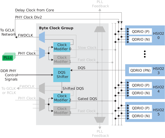
| GPIO Mode | Description |
|---|---|
| Output |
Only the output path is enabled; always registered.
Four registers capture the data on the positive edge of the slow
output clock, multiplexing them into one data stream clocked out
both edges of the fast output clock.
|
| Bidirectional |
The input, output, and OE paths are enabled; always registered.
Four registers capture the data on the positive edge of the slow
output clock, multiplexing them into one data stream clocked out
both edges of the fast output clock.
On the input side, a FIFO captures data on both edges of the input
fast clock and reads four bits of data on the positive edge of the
input slow clock.
|
| Port | Direction | Clock Domain | Notes |
|---|---|---|---|
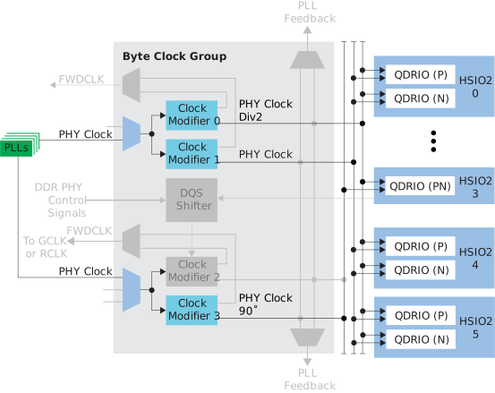
| OUTFASTCLK | Input | N/A | Byte clock signal. This signal is the TX PHY clock running at half
the data rate, and it comes from the clock modifier in the byte clock
group. If this signal is a DQ or DM bit, the phase shift is 0.
If it is the DQS bit, the phase shift is
90°. |
| OUTSLOWCLK | Input | N/A | Byte clock signal. This signal is the TX PHY clock Div2 running at one quarter the data rate. It comes from the clock modifier in the byte clock group. |
| INFASTCLK | Input | N/A | Byte clock signal. This signal is the RX PHY clock running at half
the data rate. It comes from the DQS shifter. Only available in
bidirectional mode. |
| INSLOWCLK | Input | N/A | This signal is the RX PHY clock Div2 running at one quarter the data
rate. It comes from the core, and is the forwarded clock (FWDCLK) from
the clock modifier. Only available in bidirectional
mode. |
| DLYCLK | Input | N/A | Delay clock signal from the global or regional clock network.
Only available in bidirectional mode. |
| O[3:0] | Input | OUTSLOWCLK | DQ data output synchronous to to the PHY clock Div2. |
| OE[1:0] | Input | OUTSLOWCLK | DQ data output enable synchronous to PHY clock Div2. Only
available in bidirectional mode. |
| I[3:0] | Output | INSLOWCLK | DQ data input synchronous to the PHY clock Div2 forwarded to the
core. Only available in bidirectional mode. |
| FIFO_RSTN | Input | N/A | Reset for the read FIFO. Only available in bidirectional
mode. |
| FIFO_EMPTY | Output | INSLOWCLK | Read FIFO empty. Only available in bidirectional
mode. |
| FIFO_REN | Input | INSLOWCLK | FIFO read enable. The DQS shifter drives this signal. Only
available in bidirectional mode. |
| FIFO_WEN | Input | INFASTCLK | FIFO write enable. The DQS shifter drives this signal. Only
available in bidirectional mode. |
| TERM | Input | N/A | Enable dynamic input termination. The DQS shifter drives this
signal. Only available in bidirectional mode. |
| DLY_INC | Input | DLYCLK | Dynamic delay control. 1: Increment 0: Decrement when
DLY_ENA = 1. Only available in bidirectional
mode. |
| DLY_ENA | Input | DLYCLK | Enable the dynamic delay control. Only available in bidirectional
mode. |
| DLY_RST | Input | DLYCLK | Reset the delay counter. Each HSIO2 block has one reset. Only
available in bidirectional mode. |
| DBG[5:0] | Output | DLYCLK | Debug pin. |
| ALT | Output | DLYCLK | DQS_IN clock signal that drives the DQS shifter's DQS_IN pin. |
| Signal | Direction | Description |
|---|---|---|
| IO | Bidirectional | DDR pad. TX traffic outputs on OUTFASTCLK; RX traffic inputs on INFASTCLK. |