Ti125 Power-Up Sequence
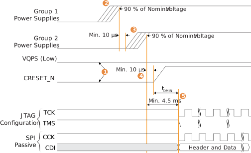
Important: You can only use one configuration channel at a time. Using SPI
passive and JTAG at the same time can result in configuration failure.
- The
CRESET_Ninput must stay low until all power supplies are powered up. Additionally,VQPSmust always stay low unless you are blowing the Ti125 security fuses.Note: Refer to Fuse Programming Requirements if you need to blow the security fuses for the Ti125 FPGA on your board. - Power up supplies in group 1 first. You can power up these supplies in any
sequence.Important: Ensure the power ramp rate is within the values shown in Table 3.
- Power up the group 2 supplies in any sequence at a minimum delay of 10 µs after group 1 supplies have reached 90% of their nominal voltage levels.
- Release the
CRESET_Ninput to high at a minimum delay of 10 µs after all FPGA supplies have reached 90% of their nominal voltage levels. - FPGA configuration can begin after there has been:
- A 4.5 ms minimum delay after all supplies have reached at least 90% of their nominal voltage.
- A tDMIN minimum delay after
CRESET_Ngoes high (see Ti125 SPI Passive Mode and Ti125 JTAG Mode for the delay specification).
Note: With the configuration bitstream stored in the SPI flash device and the SPI active hardware connection properly established, the SPI active configuration automatically starts after theCRESET_Nsignal transitions from low to high.
| Power-Up Sequence | |
|---|---|
| Group 1 | Group 2 |
| VCC VCCA |
VCCAUX
VCCIO
VCCIO33
|