Ti125 Clock and Control Network
The Ti125 FPGA has an enhanced clock network comprising global, regional, and local clocks as well as PHY clocks and byte clocks. The clock and control network is distributed through the FPGA to provide clocking for the core's LEs, memory, DSP blocks, I/O blocks, and control signals.
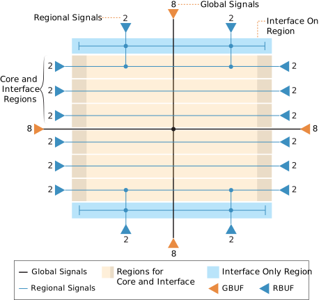
The FPGA has 32 global signals that can be used as either clocks or control signals. The global signals are balanced trees that feed the whole FPGA.
The FPGA also has regional signals that can only reach certain FPGA regions, including the top or bottom edges. The FPGA has 6 regional networks for the core, right interface, and left interface blocks. The top and bottom interface blocks have one regional clock network each. You can drive the right and left sides of each region independently. Each region also has a local network of clock signals that can only be used in that region.
The core's global buffer (GBUF) blocks drive the global and regional networks. Signals from the core and interface can drive the GBUF blocks.
Each network has dedicated enable logic to save power by disabling the clock tree. The logic dynamically enables/disables the network and guarantees no glitches at the output.
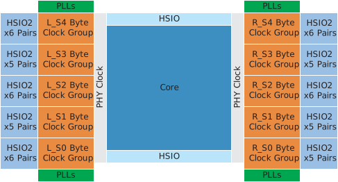
In the Ti125 FPGA, the HSIO on the top and bottom connect to the global and regional clock networks. The HSIO2 on the left and right connect to the global and regional clock networks as well as the PHY clocks and byte clock groups.