Ti125 Driving the Global Network
You can access the global clock network using the global clock GPIO pins, PLL outputs, oscillator output, clock modifiers, and core-generated clocks.
A clock multiplexing network controls which interface blocks can drive the global and regional networks. Eight of the clock multiplexers are dynamic (two on each side of the FPGA), allowing you to change which clock drives the global signal in user mode.
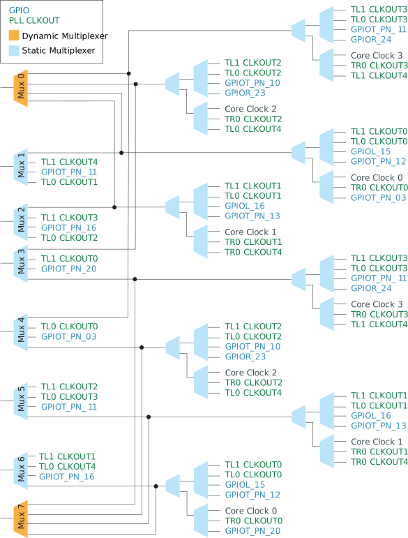
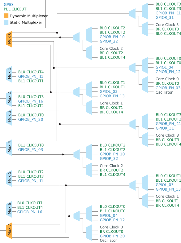
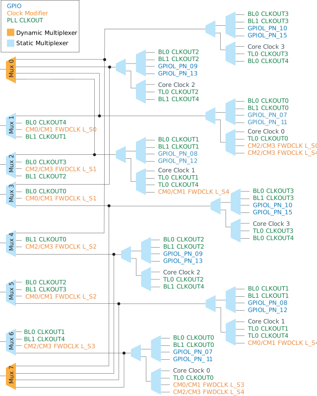
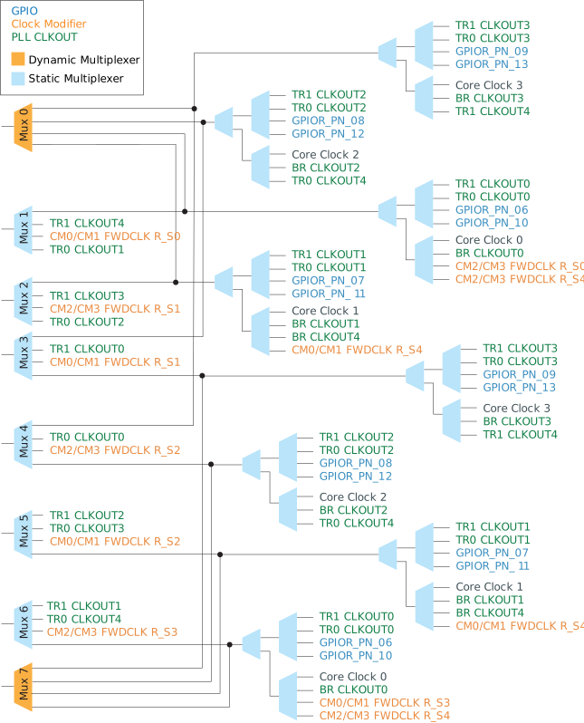
The following figure shows the global network clock sources graphically.
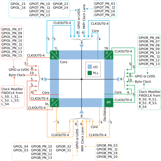
Numerous clock sources feed the global network. These signals are multiplexed together with static and dynamic clock multiplexers.
The dynamic multiplexers are configurable by the user at run-time. You can choose which clock source drives which input to the dynamic multiplexer. When you enable the dynamic multiplexer, you specify a select bus to choose which clock source is active.
When dynamically switching between the clock inputs of a dynamic multiplexer, both the currently active input and the input you intend to switch to must have toggling clocks during the switching period. Additionally, upon configuration completion and when the device transitions into user mode, input 0 of the dynamic multiplexer becomes the default active input. Therefore, you must feed a toggling clock to input 0 before switching to other inputs.
The following figures show the resources that drive each multiplexer.