Ti125 HSIO Configured as GPIO
You can configure each HSIO block as two GPIO (single-ended) or one GPIO (differential).
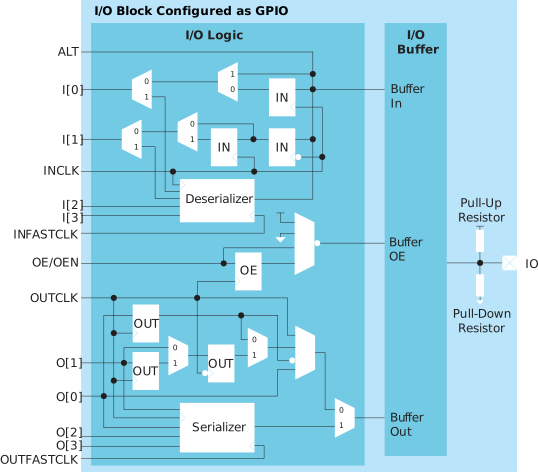
| Signal | Direction | Description |
|---|---|---|
| I[3:0] | Output | Input data from the pad to the core fabric. I[0] is the normal
input to the core. In DDIO mode, I[0] is the data captured on the
positive clock edge (HI pin name in the Interface Designer) and I[1]
is the data captured on the negative clock edge (LO pin name in the
Interface Designer). When using the deserializer, the
first bit is on I[0] and the last bit is on I[3]. |
| ALT | Output | Alternative input connection for GCLK, PLL_CLKIN, RCLK, PLL_EXTFB,
and VREF. (In the Interface Designer, Register
Option is none).
|
| O[3:0] | Input | Output data to GPIO pad from the core fabric. O[0] is the normal
output from the core. In DDIO mode, O[0] is the data output on the
positive clock edge (HI pin name in the Interface Designer) and O[1]
is the data output on the negative clock edge (LO pin name in the
Interface Designer). When using the serializer, the first
bit is on O[0] and the last bit is on O[3]. |
| OE/OEN | Input | Output enable from core fabric to the I/O block. Can be
registered. OEN is used in differential mode. Drive it with the
same signal as OE. |
| DLYCLK | Input | Delay clock for dynamic delay, sampled on the negative edge. In serializer mode, this clock must be the same clock as INCLK. |
| DLY_ENA | Input | (Optional) Enable the dynamic delay control. Assert or de-assert the signal on the falling edge of DLYCLK in your RTL design. |
| DLY_INC | Input | (Optional) Dynamic delay control. When DLY_ENA =
1, 1: Increments 0: Decrements Assert or
de-assert this signal on the falling edge of DLYCLK in your RTL
design. The updated delay count takes effect approximately 5 ns
after the rising edge of DLYCLK in the HSIO
block. |
| DLY_RST | Input | (Optional) Reset the delay counter. |
| OUTCLK | Input | Core clock that controls the output and OE registers. This clock is not visible in the user netlist. |
| OUTFASTCLK | Input | Core clock that controls the output serializer. |
| INCLK | Input | Core clock that controls the input registers. This clock is not visible in the user netlist. |
| INFASTCLK | Input | Core clock that controls the input serializer. |
| Signal | Direction | Description |
|---|---|---|
| IO (P and N) | Bidirectional | GPIO pad. |
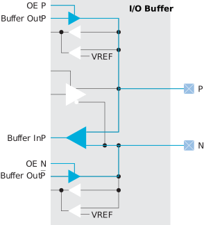
The signal path from the pad through the I/O buffer changes depending on the I/O standard you are using. The following figures show the paths for the supported standards. The blue highlight indicates the path.
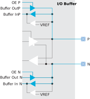
When using an HSIO with the HSTL or SSTL I/O standards, you must configure
an I/O pad of the standard's input path as a VREF pin. There is one
programmable VREF per I/O bank.
VREF pin, you must use the VREF from the same
physical I/O bank even when the I/O banks are merged to share a common VCCIO pin.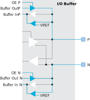
When using an HSIO with the differential HSTL or differential SSTL standard, you must use both GPIO resources in the HSIO. You use the core interface pins associated with the P resource.