Ti135 LPDDR4/4x SDRAM (N576D2F4 and N576D3F4 Only)
The Ti135 FPGA in N576D2F4 and N576D3F4 packages includes an LPDDR4/4x SDRAM device in the package. The DRAM has a density of 2 Gbits (N576D2F4) or 4 Gbits (N576D3F4) and a clock rate of up to 1,500 MHz. It supports double-data rates of up to 3,500 Mbps and has a 16-bit data bus.
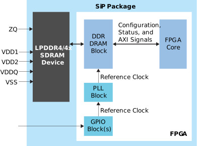
Note: The PLL reference clock must be driven by I/O pads. The Efinity software issues a warning if
you do not connect the reference clock to an I/O pad. (Using the clock tree may
induce additional jitter and degrade the DDR performance.) Refer to PLL for more information about
the PLL block.
| Name | Direction | Description |
|---|---|---|
| ZQ | Input | Calibration resistor pin. This pin calibrates the drive strength and termination resistance. Connect the ZQ pin to VDDQ through a 240 Ω ± 1% resistor. |