Ti95 HSIO2 Configured as MIPI Lane
You can configure the HSIO2 block as a MIPI RX or TX lane. The block supports bidirectional data lane, unidirectional data lane, and unidirectional clock lane which can run at speeds up to 2.5 Gbps. The MIPI lane operates in high-speed (HS) and low-power (LP) modes. In HS mode, the HSIO2 block transmits or receives data with a x8 serializer/deserializer. In LP mode, it transmits or receives data without deserializer/serializer.
- Multiple MIPI RX or TX lanes (at least a clock lane and a data lane)
- Soft MIPI D-PHY IP core programmed into the FPGA fabric
The MIPI D-PHY standard is a point-to-point protocol with one endpoint (TX) responsible for initiating and controlling communication. Often, the standard is unidirectional, but when implementing the MIPI DSI protocol, you can use one TX data lane for LP bidirectional communication.
The protocol is source synchronous with one clock lane and 1, 2, 4, or 8 data lanes. The number of lanes available depends on which package you are using. Dedicated HSIO2 blocks are assigned on the RX interface as clock lanes while the clock lane for TX interface can use any of the HSIO2 blocks in the group.
MIPI RX Lane
In RX mode, the HS (fast) clock comes in on the MIPI clock lane and is divided down to generate the slow clock. The fast and slow clocks are then passed to neighboring HSIO2 blocks to be used for the MIPI data lanes.
- One clock with four data lanes or
- One clock with one data lane and one clock with two data lanes or
- Two pairs of one clock with one data lane
Additionally, one byte clock group on each side of the FPGA can be cascaded with the neighboring byte clock group to build an eight-lane interface. You only need to use one HSIO2 as the MIPI RX clock lane for both cascaded groups. See Cascaded MIPI Clock Lanes.
The MIPI RX function is defined as:
| MIPI RX Function | Description |
|---|---|
| RX_DATA_xy_L_Sz RX_DATA_xy_R_Sz |
MIPI RX Data Lane. x = P or N y =
data lane number, 0 - 5 (Up to 4 data lanes in one byte clock
group; up to 8 data lanes when cascading, see Cascaded MIPI Clock Lanes) z = MIPI byte
clock group number, 0 - 4 (five byte clock groups on the left
and right sides) |
| RX_CLKn_x_L_Sz RX_CLKn_x_R_Sz |
MIPI RX Clock Lane. n is the clock
number x = P or N z = MIPI
byte clock group number, 0 - 4 (five byte clock groups the left
and right sides) |
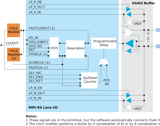
| Signal | Direction | Clock Domain | Description |
|---|---|---|---|
| LP_P_OE | Input | – | (Optional) LP output enable signal for P pad. |
| LP_P_OUT | Input | – | (Optional) LP output data from the core for the P pad. Used if the data lane is reversible. |
| LP_P_IN | Output | – | LP input data from the P pad. |
| CLKOUT | Output | – | Divided down parallel (slow) clock from the pads that can drive the core clock tree. Used to drive the core logic implementing the rest of the D-PHY protocol. It should also connect to the FIFOCLK of the data lanes. |
| SLOWCLKOUT1 | Output | – | Divided down parallel (slow) clock from the pads. Can only drive RX DATA lanes. |
| FASTCLKOUT1 | Output | – | Serial (fast) clock from the pads. Can only drive RX DATA lanes. |
| HS_IN[15:0] | Output | SLOWCLK | High-speed parallel data input. |
| FIFO_EMPTY | Output | FIFOCLK | (Optional) When the FIFO is enabled, this signal indicates that the FIFO is empty. |
| FIFO_RD | Input | FIFOCLK | (Optional) Enables FIFO to read. |
| RST | Input | FIFOCLK SLOWCLK |
(Optional) Asynchronous. Resets the FIFO and serializer. If the FIFO is enabled, it is relative to FIFOCLK; otherwise it is relative to SLOWCLK. |
| FIFOCLK1 | Input | – | (Optional) Core clock to read from the FIFO. |
| SLOWCLK1 | Input | – | Parallel (slow) clock. |
| FASTCLK1 | Input | – | Serial (fast) clock. |
| DLY_INC | Input | SLOWCLK | (Optional) Dynamic delay control. When DLY_ENA is 1, 1:
Increments 0: Decrements |
| DLY_ENA | Input | SLOWCLK | (Optional) Enable the dynamic delay control. |
| DLY_RST | Input | SLOWCLK | (Optional) Reset the delay counter. |
| LP_N_OE | Input | – | (Optional) LP output enable signal for N pad. |
| LP_N_OUT | Input | – | (Optional) LP output data from the core for the N pad. Used if the data lane is reversible. |
| LP_N_IN | Output | – | LP input data from the N pad. |
| HS_ENA | Input | – | Dynamically enable the differential input buffer when in high-speed mode. |
| HS_TERM | Input | – | Dynamically enables input termination high-speed mode. |
The clock lane generates the fast clock and slow clock for the RX data lanes within the interface group. It also generates a clock which is divided by 4 or 8 that feeds the global network. The following figure shows the clock connections between the clock and data lanes.
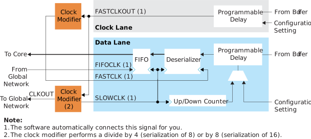
Cascaded MIPI Clock Lanes
The HSIO2 block supports clock cascading. You can cascade the clock lane from one byte clock group to another byte clock group, which allows you to have eight MIPI RX data lanes (x8) and one (cascaded) MIPI RX clock lane. The HSIO2 supports cascading for the following groups:
| MIPI RX Clock Lane | Group | Cascaded Group |
|---|---|---|
| RX_CLK0_P_R_S2, RX_CLK0_N_R_S2 | R_S2 | R_S1 |
| RX_CLK0_P_L_S2, RX_CLK0_N_L_S2 | L_S2 | L_S1 |
MIPI TX Lane
In TX mode, a PLL generates the parallel and serial clocks and passes them to the clock and data lanes.
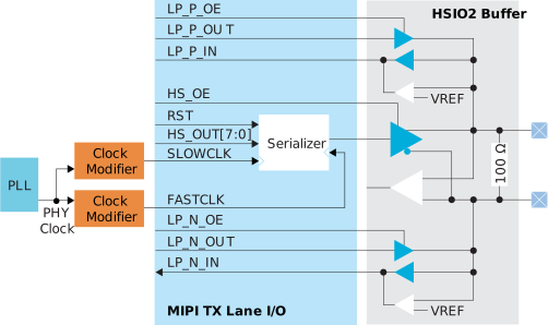
| Signal | Direction | Clock Domain | Description |
|---|---|---|---|
| LP_P_OE | Input | – | LP output enable signal for P pad. |
| LP_P_OUT | Input | – | LP output data from the core for the P pad. |
| LP_P_IN | Output | – | (Optional) LP input data from the P pad. Used if data lane is reversible. |
| HS_OE | Input | – | High-speed output enable signal. |
| RST | Input | SLOWCLK | (Optional) Resets the serializer. |
| HS_OUT[15:0] | Input | SLOWCLK | High-speed output data from the core. Always 8-bits wide. |
| SLOWCLK | Input | – | Parallel (slow) clock. |
| FASTCLK | Input | – | Serial (fast) clock. |
| LP_N_OE | Input | – | LP output enable signal for N pad. |
| LP_N_OUT | Input | – | LP output data from the core for the N pad. |
| LP_N_IN | Output | – | (Optional) LP input data from the N pad. Used if data lane is reversible. |
MIPI Lane Pads
| Signal | Direction | Description |
|---|---|---|
| P | Bidirectional | Differential pad P. |
| N | Bidirectional | Differential pad N. |