Byte Clock Groups
The PLL clock output can feed the PHY clock network. The PHY clock delivers high-speed clocks to byte clock groups, which performs clock management (division, phase shift, and delay) before the clock signal reaches the HSIO2 blocks. Byte clock groups have either five or six HSIO2 blocks.
One byte clock group on each side of the device can cascade a clock signal to the adjacent group. S2 (x6 group) can cascade to S1 (x5 group) (see Cascaded MIPI Clock Lanes).
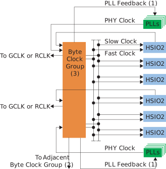
- The byte clock groups next to the PLLs can feed back to the PLL.
- Only one byte clock group on each side can cascade to the adjacent byte clock group.
- Refer to Figure 3 for details.
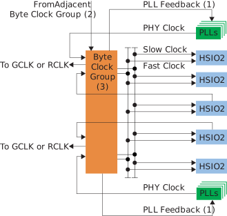
- The byte clock groups next to the PLLs can feed back to the PLL
- Only one byte clock group on each side can receive the cascaded signal from the adjacent byte clock group.
- Refer to Figure 3 for details.
Each byte
clock group has four clock modifiers (CM0 - CM3) that generate fast and slow clocks.
These clocks connect to the HSIO2 and can feed back to the global or regional clock
networks (FWDCLK signal). Each clock modifier has a clock divider and a
phase shifter. FWDCLK uses the divider; the fast/slow clocks use the
divider and phase shifter.
In QDRIO mode, the DQS shifter handles the DDR PHY control signals for read operations.
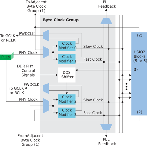
- Only one byte clock group on each side can cascade to the adjacent byte clock group.
- Only the top and bottom byte clock groups on each side can feed back to the PLL
- Refer to Ti95 HSIO2 Configured as QDRIO for the DDR PHY read and write clocking.
| Port | Direction | Notes |
|---|---|---|
| CLKIN | Input | Input clock signal from the PHY clock or a dedicated input from the HSIO2 pin. |
| CLKOUT | Output | Clock output signal that can feed the HSIO2 fast clock and slow clock. |
| FWDCLK | Output | Forward clock. This signal drives the global or regional clock network. |
| Port | Direction | Clock Domain | Notes |
|---|---|---|---|
| CLK | Input | – | Forward DIV2 clock used for DDR read tansactions. |
| DQS_IN | Input | – | DQS strobe clock from the DQS pin. |
| RD_ENABLE | Input | CLK | DQ byte read enable. |
| DQS_INVERT | Input | CLK | Optional signal to invert the DQS signal. |
| DQS_SHIFT[4:0] | Input | CLK | Control signal to tell the QDRIO when to start writing to the FIFO.
Indicates the clock cycle shift. 00000: 1 phy_clk_div2 cycle
shift 00001: 1.5 phy_clk_div2 cycle shift 00010:
2 phy_clk_div2 cycle shift 00011 2.5 phy_clk_div2
cycle_shift . . . 11111: 16.5 phy_clk_div2
cycle_shift |
| FIFO_SHIFT[1:0] | Input | CLK | Control signal to tell the QDRIO when to start reading from the FIFO.
Indicates the clock cycle shift. 00: 1 phy_clk_div2 cycle shift
from dqs_en 01: 2 phy_clk_div2 cycle shift from
dqs_en 10: 3 phy_clk_div2 cycle shift from dqs_en 11:
4 phy_clk_div2 cycle shift from dqs_en |
| DQS_DLY[3:0] | Input | CLK | DQS delay. 16 steps of 50 ps delay for the RD_ENABLE signal. |
| FIFO_RE_OUT | Output | CLK | FIFO read enable to the QDRIO. |
| FIFO_WE_OUT | Output | CLK | FIFO write enable to the QDRIO. |
| TERM_OUT | Output | CLK | Termination signal to the QDRIO. |
| RVALID | Output | CLK | Read valid. |
| DQS_OUT | Output | – | Gated DQS clock used when reading the FIFO. |