Designing with Efinix FPGA DSP Blocks
April 17, 2026
Today’s most advanced digital signal processing (DSP) solutions demand speed, adaptability, and precision — and that’s exactly where FPGAs (Field-Programmable Gate Arrays) shine. As a powerful hardware platform, FPGAs deliver exceptional parallel processing capability, high configurability, and real-time flexibility, making them an ideal solution for accelerating next-generation signal processing applications.
As a leading company in this field, Efinix offers the 40 nm Trion® series and 16 nm Titanium™ series FPGAs, each designed to address different performance tiers for DSP applications. These devices offer strong support for a wide range of real-time signal processing tasks through highly efficient DSP hardware primitives
In an FPGA, DSP primitives are dedicated hardware building blocks used to implement digital signal processing operations efficiently. These primitives commonly support functions such as multiplication, addition, accumulation, and shifting.
Compared with traditional CPUs, FPGAs can process multiple signal streams in parallel at the hardware level, offering significant advantages in performance and energy efficiency for high-throughput, low-latency applications such as audio processing, image processing, communication systems, radar, and satellite systems.
This article analyzes the architecture and functional features of Efinix FPGA DSP blocks and their application in practical designs, demonstrating how these hardware resources can be leveraged to implement efficient signal processing systems.

Introduction to Trion® Series DSP Block Primitive
The Trion® series, built on a 40nm process, features DSP modules that can operate at a maximum frequency of 400 MHz and support 18×18-bit hardware multiplication, making them suitable for moderately complex digital signal processing tasks. Refer to the respective device datasheet for their operating frequency.
EFX_MULT Primitive:
The DSP is a module within the FPGA, with input and output signals as well as some configurable parameters. The following figure shows the block diagram of the Trion® DSP primitive:
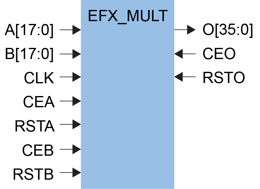
The following table provides the details for each port of the EFX_MULT primitive:
| Port Name | Direction | Description |
|---|---|---|
| A[17:0] | Input | Operand A |
| B[17:0] | Input | Operand B |
| CLK | Input | Clock |
| CEA | Input | Clock enable for A |
| RSTA | Input | Set/reset for A |
| CEB | Input | Clock enable for B |
| RSTB | Input | Set/reset for B |
| O[35:0] | Output | Multiplier Output |
| CEO | Input | Clock enable for O |
| RSTO | Input | Set/reset for O |
Refer to the Quantum Trion Primitives User Guide for more details on EFX_MULT primitive.
Summary:
The Efinix 40nm Trion® series FPGA includes an 18×18-bit hardware multiplier within its DSP module. To use this feature, simply instantiate the multiplier according to the functional block diagram.
Advanced Features of the Titanium™ Series DSP Block Primitives
With an understanding of the Efinix Trion® DSP block primitive, it becomes easier to grasp the Titanium™ DSP module. The Efinix Titanium series is manufactured using 16nm process technology, which allows its DSP to reach a peak frequency of 1000 MHz. Refer to the respective device datasheet for their operating frequency.
The Titanium™ Series FPGA offers higher performance and more advanced DSP modules than the Trion® series DSP. It supports multiplication, addition, subtraction, accumulation, and 4-bit variable right-shift operations. With multiple operating modes available, the device provides enhanced computational flexibility and parallel processing capability. Each DSP module includes four operating modes that support the following multiplication operations:
- Normal Mode—Supports one 19 x 18 integer multiplication with 48-bit addition/subtraction.
- Dual Mode—Supports one 11 × 10 integer multiplication and one 8 × 8 integer multiplication with two 24-bit addition/subtraction operations.
- Quad Mode—Supports one 7 × 6 integer multiplication and three 4 × 4 integer multiplications with four 12-bit addition/subtraction operations. (Note: the output of the 7 × 6 Quad mode will be truncated to 12-bit.)
- Float Mode—Supports one fused-multiply-add/subtract/accumulate (FMA) BFLOAT16 floating-point multiplication.
The multiplier/adder can operate under either SIGNED/UNSIGNED mode according to value of the SIGNED-parameter. When multiple fractured, e.g., EFX_DSP12 / EFX_DSP24, operators are to be mapped onto the same physical EFX_DSP48 instance, they must share the same SIGNED-parameter value. The multiplier inputs can be A and B, and the output result can be used for addition or subtraction operations.
EFX_DSP48 Primitive Overview
The following figure shows the block diagram of Titanium™ DSP Block.
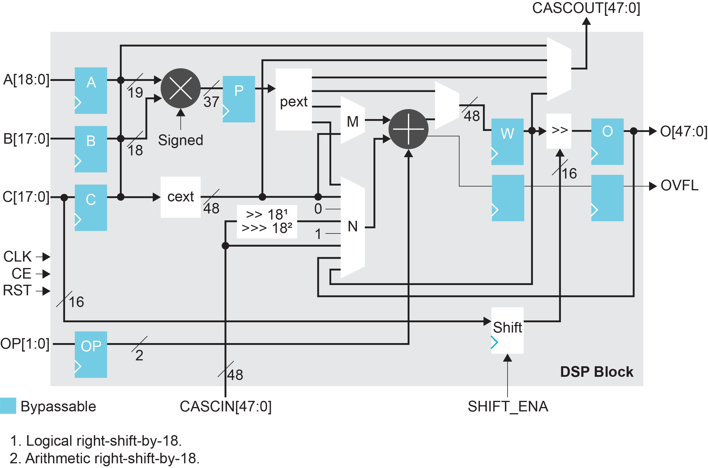
The registers in blue colour are bypassable. The DSP block includes a 19 × 18-bit signed/unsigned multiply-accumulate unit with a 37-bit output. This output is optionally registered by the P register (which can be enabled or bypassed by the user) before propagating to pext. pext is used to extend the 37-bit output to 48 bits, with two options below:
- ALIGN_LEFT: Left-aligned, with zero-padding on the right.
- ALIGN_RIGHT: Right-aligned, with sign extension, where the leftmost bits are filled with the sign bit (0 or 1).
pext is connected to multiple outputs. For example, it can pass through an M multiplexer to enter the adder module, or it can select the CASCOUT output through CASCOUT_SEL.
If the output is routed to the adder module, M_SEL and N_SEL select the two adder inputs, while OP[1:0] determines the adder operation (as described in the signal description table below). The adder result can then be routed to the W register via W_SEL and is ultimately output through the O register.
The EFX_DSP48 primitive supports the full functionality of the DSP blocks in all modes (NORMAL, DUAL, QUAD and BFLOAT). The following figure is the signal block diagram of the EFX_DSP48 primitive with a detailed signal description table. You can refer to the corresponding description and the DSP block architecture figure above for better understanding.
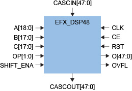
| Port Name | Direction | Description |
|---|---|---|
| A[18:0] | Input | Operand A. |
| B[17:0] | Input | Operand B. |
| C[17:0] | Input | Operand C. |
| OP[1:0] | Input | Add/subtract function control. 00: M + N 11: M - N 10: -M + N 11: -M - N |
| SHIFT_ENA | Input | Load the shifter register S from the C input. |
| CASCIN[47:0] | Input | Dedicated input from the DSP block below. |
| CLK | Input | Clock. |
| CE | Input | Clock enable. |
| RST | Input | Reset. |
| O[47:0] | Output | DSP Output. |
| CASCOUT[47:0] | Output | Dedicated output to the DSP block above. |
| OVFL | Output | Overflow/underflow flag. Signed—The operation behaves as you would expect. Unsigned—When OP is 00, the operation behaves as you would expect. For the other operands, it reports overflow or underflow if information is lost during the operation. When using dual or quad mode, the overflow bits are calculated independently and ORed together. |
EFX_DSP48 Operational Modes
Normal Mode
- Function—Performs 19 × 18 integer multiplication, producing a 37-bit result (P), which can be extended to 48 bits. The multiplier supports both signed and unsigned operations, controlled by the SIGNED parameter.
- Extension and Shifting—The C input is 18 bits, which can be extended to 48 bits via the C_EXT parameter. The logical shifter supports right shifts from 0 to 15 bits, with the shift type (arithmetic or logical) depending on the DSP block's sign setting. The shift value is captured from the C input when enabled by the SHIFT_ENA port.
- Applicable Scenarios—Applications that requires high-precision multiplication, such as filter design or large accumulation operations.
Dual Mode
- Function—Simultaneously performs an 11 × 10 multiplication (21-bit result) and an 8 x 8 multiplication (16-bit result), both extended to 24 bits.
- Data Path—The C input is allocated to two separate data paths, each of which can be independently extended. The shifting function is similar to the Normal mode, supporting dynamic shift control.
- Applicable Scenarios—Signal processing with moderate parallelism, such as dual-channel audio processing or pixel operations in image processing.
Quad Mode
- Function—Performs a 7 × 6 multiplication (13-bit result, truncated to 12 bits) and three 4 × 4 multiplications (8-bit results, extended to 12 bits). Note: The 7 × 6 multiplication result is truncated, so the calculation range is limited.
- Special Handling—The C input is divided into four separate data paths. The shifter supports independent shifting for multiple channels, enhancing flexibility.
- Applicable Scenarios—High-parallelism, low-precision tasks, such as weight calculations in machine learning or multi-channel sensor data processing.
Float Mode
- Function—Supports BFLOAT16 format fused multiply-add (FMA) operations, with input in BFLOAT16 and output in FP32 format. This mode is specifically optimized for AI and machine learning applications.
- Configuration Requirements—Registers such as A_REG, B_REG, P_REG, OP_REG, and W_REG must be enabled, and P_EXT and C_EXT should be set to ALIGN_RIGHT. The shifter is bypassed.
- Output Format—The O output includes error flags (such as overflow, invalid operation), with bits [31:0] representing FP32 data.
- Applicable Scenarios—Floating-point intensive applications, such as neural network inference or scientific computing.
When using the Efinix Titanium™ Series DSP primitives, the designer should select the operating mode based on operand bit-width requirements to ensure optimal resource efficiency and minimal DSP block utilization. Refer to the Quantum Titanium Primitives User Guide for more details on the Titanium DSP block primitives.
Conclusion
The DSP blocks in Efinix FPGAs span from the 18 × 18 fixed-point multiplier in the Trion® series to the high performance 1000MHz multi-mode configurable DSP block in the Titaniun™ Series, demonstrating continuous optimization and innovation in hardware acceleration.
For applications ranging from low to medium complexity embedded processing to high throughput, multichannel real-time signal processing, designers can maximize the usage of these DSP blocks through strategic selection and configuration. This enables them to fully leverage the performance, power efficiency, and flexibility of Efinix FPGAs to develop efficient and reliable digital signal processing systems.
With a structured overview of the architecture, supported features, and application methods of Efinix DSP blocks, designers can gain a deeper understanding of how they work and how to apply them effectively in real world designs, enabling the development of more powerful and efficient signal processing solutions.