
Newsroom > Blog
March 07, 2023
As discussed in our blog article “RISC-V and FPGAS” RISC-V is not a new open standard, but its adoption is now accelerating thanks to the number of open developer resources and support from major semiconductor vendors. This open standard is democratizing chip design, but adding some custom instructions to a standard RISC-V core allows the designer to really take advantage of the benefits of the RISC-V architecture.
The most important advantage of RISC-V for a systems developer is the fact that RISC-V is open source. The RISC-V source can be accessed by anyone and used as the foundation for a new hardware implementation of a base instruction set architecture (ISA) for a new processor. Traditionally this is very difficult or not allowed with proprietary ISAs that are acquired under license. Starting with an open-source standard is the fastest way to begin developing specialty logic for core architectures and the corresponding hardware implementation. The Efinix Sapphire core is an example of one such open source RISC-V implementation. A version of Sapphire is freely available on the Efinix Github while a fully configurable version is available to use with the graphical user interface of the IP Manager within the Efinity toolset.
While RISC-V can be used as a standalone core architecture that can be ported to run Linux kernels, adding custom instructions on top of RISC-V can help accelerate particular algorithms. The Sapphire core is fully Linux compatible and can be instantiated in up to four core configurations for added processing while retaining full custom instruction compatibility. In this article, we’ll provide an overview of the Sapphire custom instruction capability.
The workflow for developing custom instructions for a RISC-V implementation is very similar to what is used in software engineering workflows generally. The Sapphire core resembles a traditional processor core with the associated ALU. Additionally, however, Sapphire contains a custom instruction interface block that provides for two 32-bit source registers and a single 32-bit destination register along with a 10 bit function code and four control signals to control handshaking of data between the core and an externally defined custom ALU. Four opcodes in the RISC-V ISA are available for custom instructions namely, 0x0B, 0x2B, 0x5B and 0x7B. Each opcode can be further extended with the 10 bit function code giving 1024 effective instructions for each opcode.
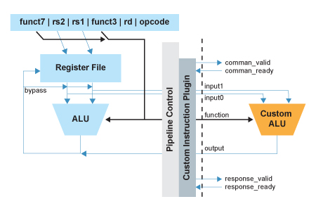
Figure 1: The Sapphire Custom Instruction Interface
The first step in implementing custom instructions in RISC-V is to create the user defined ALU that will execute the instructions. Having a pre-defined interface between the RISC-V core and the new ALU means that a common template for the new ALU can be defined. Examples of this ALU definition in RTL are readily available on the Efinix Github within the TinyML section and can be used as templates for a user defined ALU. All that is required of the designer is to write a small block of RTL to implement the function to be accelerated and drop that into the supplied template. Again, examples of simple instructions are provided on the Efinix Github pages to guide the designer.
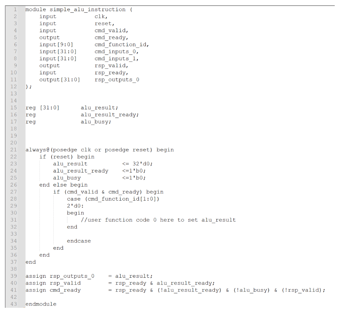
Figure 2: The Sapphire Custom Instruction Interface (Code Fragment for Reference Only)
Here we see a simplified RTL template for the user-defined ALU. Input and output signals are defined for the module in lines 1 through 12. The main body of the ALU (once reset into a known state) waits for the command valid and ready signals and then samples the value of the command function. A case statement selects a valid operation depending on the value of this function extension. On lines 30-32, we see a Begin–End pair that surround the area that would contain the designer’s expression for a function extension value of zero. Once the designer’s expression has been evaluated, the result is passed back to the main RISC-V core in the rsp_outputs_0 variable using the handshaking established for the standard template.
Now that we have hardware implementations of the desired custom instructions instantiated in the Efinity project, it only remains to call them from within the application code running on the RISC-V processor. Fortunately, this too is straight forward due to the presence of inline assembly instructions in the C programming language.
Within the RISC-V application code, a macro can be defined that formats the required opcode, function ID, source and destination registers into the format expected by the custom instruction control interface and inserts the formatted instruction in an inline assembly call.
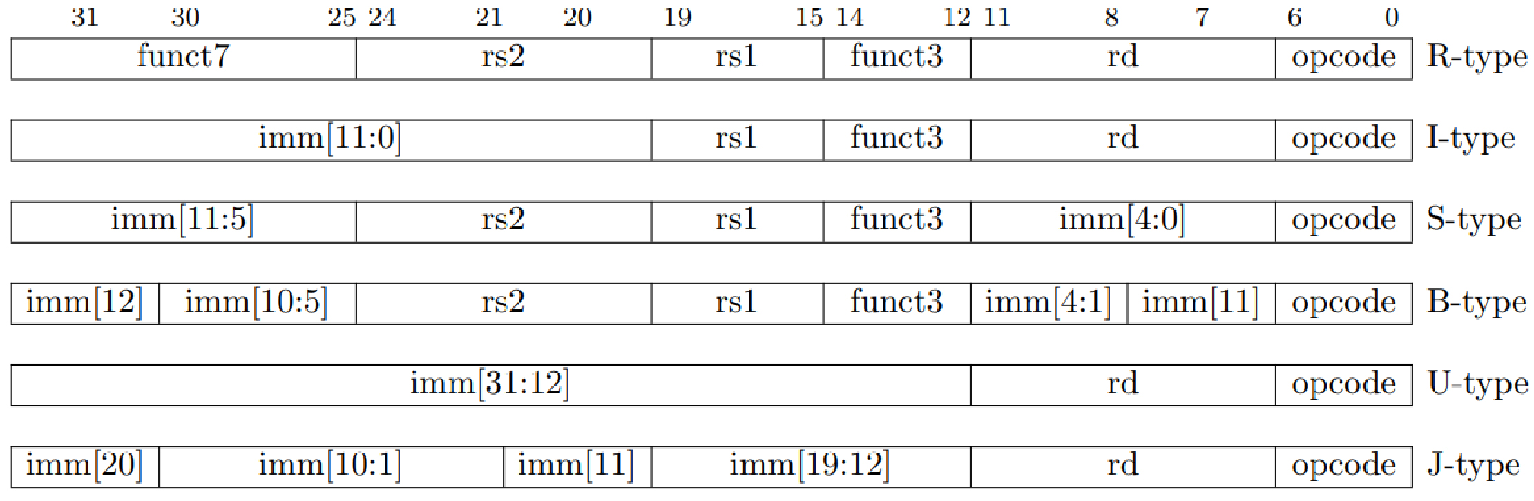
Figure 3: Structure of RISC-V Instructions
Source: RISC-V Instruction Set Manual
Here we see the format of various RISC-V instructions. We will use the R-Type function and will format the 32-bit value with bits representing the Opcode and the required function extension value (zero for the example custom ALU template provided above).
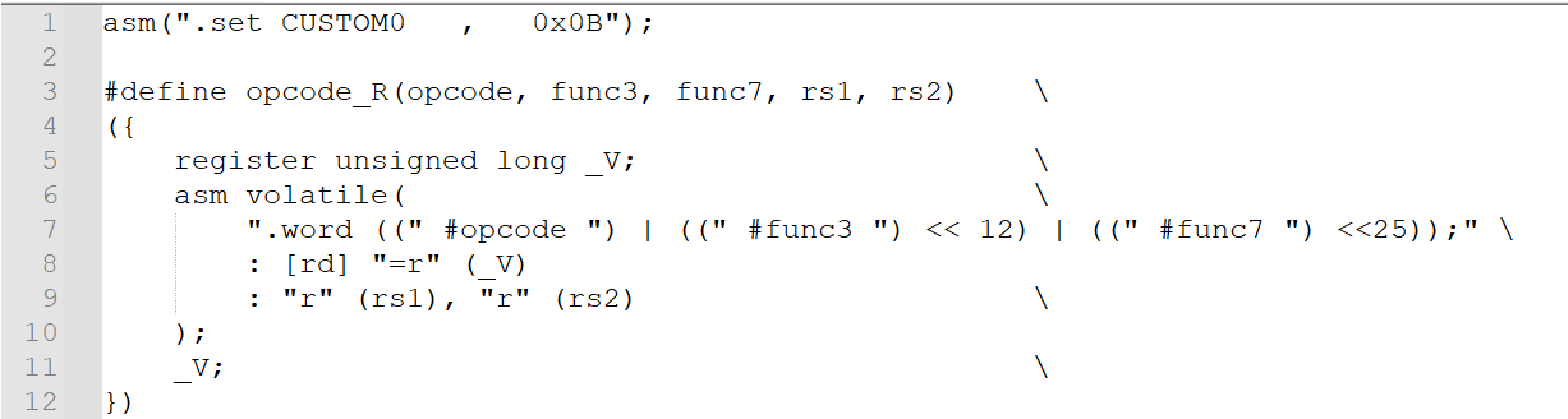
Figure 4: Macro to Format a Custom Instruction for Inline Assembly (Code Fragment for Reference Only)
We append the register that will be used as source and destination registers for the custom instruction interface block and define the opcode of the custom instruction we will be using, in this case 0x0B.
Now that we have opcode_R defined, we can use it to call an inline assembly instruction passing two 32 bit registers to our custom ALU and returning a 32 bit register of result. For example, in our application code, if we were to define a function call as follows;
#define my_instruction (rs1, rs2) opcode_R (CUSTOM0, 0x00, 0x00, rs1, rs2)
We can now call my_instruction (num1, num2) with two unsigned integers as operands, implicitly use custom instruction 0x0B and function ID 0x00, and retrieve an unsigned integer as a result from our newly defined custom ALU.
We see here how, using an Efinix FPGA and the open source Sapphire core, it becomes extremely easy to define and call custom instructions that take 8 bytes of input data and return four bytes of the result. Using this technique, complex operations can be defined within the custom ALU that operate at hardware speed and result in massive acceleration at an application level. The technique is easy to apply and iterate. Results can rapidly be observed as system performance is progressively accelerated. The main application remains in software where it can be rapidly developed and evolved using traditional software techniques while key aspects of the design can be accelerated at hardware speed delivering improved system level performance.
For a full walkthrough of these techniques and how they can be applied to massively accelerated machine learning, go to the Efinix GitHub page for our TinyML accelerator and follow along with the tutorial for TinyML acceleration.
As a closing thought, since the custom ALU that we have defined is resident in the FPGA fabric and can have both state and arbitrary complexity, there is nothing to stop us from giving our two source registers meaning other than their face value. We could for example use them as pointer to larger data structures or use them to control the flow of data in other areas of the FPGA opening up the possibility of much larger functionality for our custom ALU and the potential of massive application acceleration under application control. Similarly, we could define multiple custom instructions and use them to pass multiple operands and conduct algorithms with greater parallelism. Again, see out TinyML Github pages for examples of how more complex custom ALU definitions can be applied to machine learning acceleration.
In this tutorial, we have shown how FPGAs and the RISC-V processor are ideal companions. The extensible nature of the RISC-V architecture sits naturally alongside (or within) an FPGA where the FPGA can be used to quickly instantiate the additional hardware, extending the RISC-V’s feature set at hardware speed. The beauty of designing with the Sapphire RISC-V core inside Efinix FPGAs is that ample room is available in the FPGA alongside the instantiated Sapphire core to implement whatever custom instructions are needed. The flexible nature of the FPGA means that instructions can be added or iterated as needed to achieve the desired system performance. Design cycles are extremely short and the results of the custom instruction acceleration on system performance can be quickly observed.