JTAG to SPI Flash Bridge Core
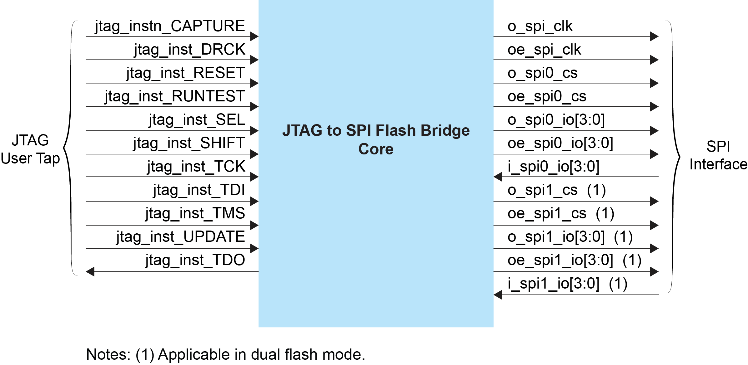
The JTAG to SPI Flash Bridge core is an enhanced version of the JTAG SPI Flash Loader core, designed to provide seamless access to the SPI flash memory through a JTAG header on a computer. With this core, you can use the JTAG interface to program the configuration bitstream into the SPI flash memory. Once programmed, the FPGA can be reconfigured using the SPI Active mode.
Unlike its predecessor, the JTAG to SPI Flash Bridge core eliminates the need for an additional clock. It relies solely on the TCK clock, which generates all the necessary signals. This reduces the clock buffer usage, simplifies design complexity, and makes it easier to meet timing constraints. Additionally, it features an on-chip CRC32 calculation, enabling verification directly within the FPGA instead of relying on the host PC for read comparisons.
JTAG to SPI Flash Bridge Block Diagram
Features
- Verilog RTL and simulation testbench
- Include example design targeting the:
- Trion T120 BGA324 Development Board
- Titanium Ti60 F225 Development Board
- Titanium Ti180 J484 Development Board
- Titanium Ti375 C529 Development Board
User Guide