PCIe Scatter-Gather Direct Memory Access (SGDMA) Core
The SGDMA IP enables data transfer between the host memory and FPGA user logic via the PCIe interface. It supports two transfer modes:
- Host-to-Card (HTC)
- Card-to-Host (CTH)
Both modes support bidirectional data transfer between the FPGA and the host. Using a chained descriptor queue mechanism, the SGDMA engine efficiently and flexibly handles data transfer tasks.
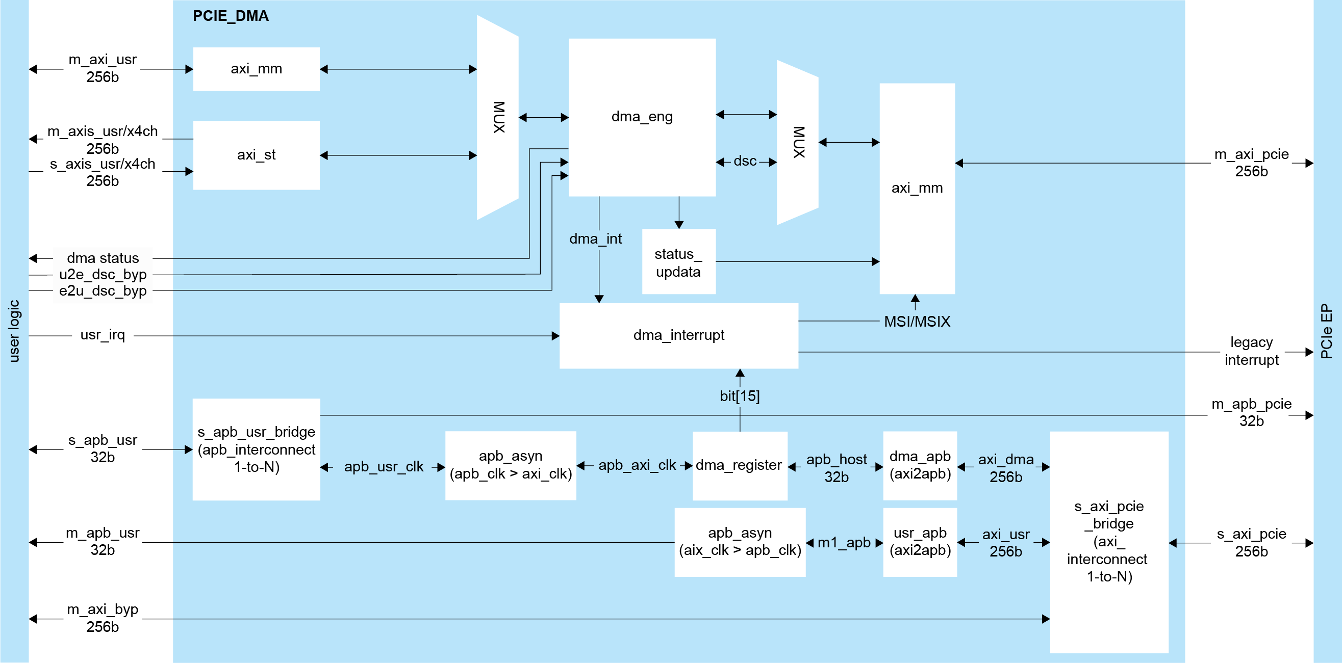
SGDMA Block Diagram
Features
- Data transfer using the standard AXI4-MM protocol
- Data transfer in AXI4-Stream mode
- Master APB3 interface for host-to-card register configuration
- Slave APB3 interface for user logic-to-IP register configuration
- Legacy and MSI-X interrupts
Additionally, the PCIe SGDMA Core supports the following features:
| Feature | Efinix PCIe SGDMA IP |
|---|---|
| Data Width | 256 bits |
| Host-to-Card | Up to four channels |
| Card-to-Host | Up to four channels |
| Descriptor Engine Pause Control | Supported |
| AXI-MM Bypass Interface | Supported |
| Descriptor | Up to 256 MB data length per descriptor |
| Write Back/Polling | Supported |
| Legacy INTX | Single channel (INTA only) |
| User INTR | INTA MSIX MSI |
| MSIX | Supported |
| MSI | Supported |
| MPS, MRRS | MPS=128, 256, 512 MRRS=128, 256, 512, 1024, 2048, 4096 Measured in bytes |
| Clock Frequency | AXI clock = {125 to 250} MHz APB clock = {20 to 200} MHz Must use same CLK source as PCIe EP |
| APB Interface | Supported |
| AXI4-MM Interface | Supported |
| AXI4-Stream interface | Supported |