MIPI DSI RX Controller V2 Core
The MIPI DSI specifies the physical link between the chip and display in devices such as smartphones, tablets, AR/VR headsets and connected cars. It defines a serial bus and a communication protocol between the host, the source of the image data, and the destination, for example, display peripherals. The MIPI DSI RX Controller V2 core implements the MIPI DSI interface in the FPGA and lets you configure the related parameters.
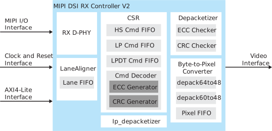
MIPI DSI RX Controller V2 Block Diagram
Features
- Supports 1, 2, and 4 lanes
- Supports continuous or discontinuous clock mode
- IP core clock frequency at 100 MHz
- PHY Protocol Interface (PPI) that supports 8-bit or 16-bit high-speed transmitting data bus
- Supports data rate: (1)
- PPI 8-bit—Up to 1.5 Gbps (HS mode byte clock frequency from 10 MHz up to 187 MHz)
- PPI 16-bit—Up to 2.5 Gbps (HS mode byte clock frequency from 5 MHz up to 156 MHz)
- Includes AXI4-Lite interface for register access
- Error correction code (ECC) generation for packet headers
- Cyclic redundancy check (CRC) generation for data bytes
- Supports non-burst with sync pulses, non-burst with sync events, and burst mode
- Supports command transmission in HS or LP mode
- Supports initial skew calibration after initialization is completed
- Supports all Titanium and Topaz FPGAs
Note: 1) The maximum data rate of IP depends on the devices. Refer to the respective device data sheet for more accurate information.