MIPI CSI-2 TX Controller V2 Core
The MIPI CSI-2 interface, which defines a simple, high-speed protocol, is the most widely used camera interface for mobile. Adding a MIPI interface to an FPGA creates a powerful bridge for transmitting or receiving high-speed video data easily to or from an application processor. The MIPI CSI-2 TX Controller V2 core enables complex video and image processing as part of a complete system solution.
MIPI CSI-2 TX Controller V2 Block Diagram
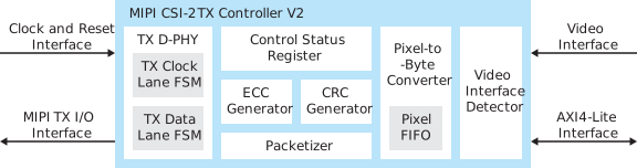
Features
- Configurable data lanes: 1, 2, 4, or 8
- High-speed (HS) mode and Low-power (LP) mode
- Arbitrary number of payload data bytes
- PHY Protocol Interface (PPI) that supports 8-bit or 16-bit high speed transmitting data bus
- Supports data rate: (1)
- PPI 8-bit—Up to 1.5 Gbps (HS mode byte clock frequency from 10 MHz up to 187 MHz)
- PPI 16-bit—Up to 2.5 Gbps (HS mode byte clock frequency from 5 MHz up to 156 MHz)
- Continuous HS mode byte clock and discontinuous HS mode byte clock
- Pixel format :
- RAW: RAW6, RAW7, RAW8, RAW10, RAW12,RAW14, RAW16, RAW20, RAW24, RAW28
- RGB: RGB444, RGB555, RGB565, RGB888
- YUV: YUV420 8-bit (legacy), YUV420 8-bit, YUV420 10-bit, YUV420 8-bit (CSPS)
- YUV420 10-bit (CSPS), YUV422 8-bit, YUV422 10-bit
- User defined 8-bit data types
- Generic 8-bit long packet
- Null, blank, and embedded 8-bit non-image data
- Generic frame mode and accurate frame mode
- Supports end-of-transmission error, start-of-transmission sync error, control error and LP escape error
- Supports control status register (CSR) for status and error assertion accessed through AXI4-Lite interface
- Supports initial skew calibration after initialization is completed
- Supports all Titanium and Topaz FPGAs
User Guide