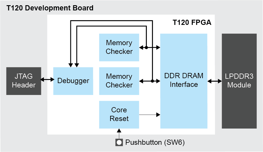
Example Design: Trion T120 BGA324 DDR Read/Write Test
This simple design demonstrates a project using the T120 BGA324 FPGA's DDR interface. It performs a simple read/write test for the LPDDR3 memory chip on the Trion® T120 BGA324 Development Board.
This design was compiled with Efinity® software v2020.1 and targets the Trion® T120 BGA324 Development Board.
This content is locked and requires you to login before viewing more.