Titanium™ Ti85 FPGAs
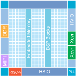
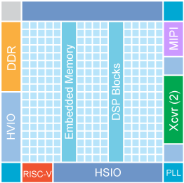
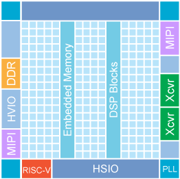
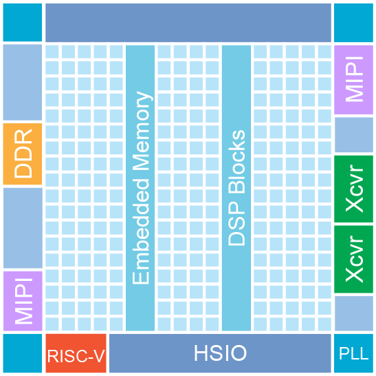
The Ti85 FPGA features the high-density, low-power Efinix® Quantum® compute fabric wrapped with an I/O interface. This FPGA has a variety of features, such as a hardened RISC-V block, transceivers (includng PCIe® Gen 4x4), LPDDR4/4x DRAM controller, and MIPI D-PHY.
The quad-core hardened RISC-V block has a 32-bit CPU featuring the ISA RISCV32I with M, A, C, F, and D extensions, and six pipeline stages. You utilize the hardened RISC-V block by instantiating the Sapphire High-Performance SoC, combining the speed and efficiency of a hardened RISC-V block with the flexibility of peripherals in soft logic.
The full-duplex transceiver supports the PCIe 4.0, Ethernet SGMII, and Ethernet 10GBase-KR protocols as well as a PMA direct mode with data rates up to 12.5G.
Ti85 FPGAs include a hardened MIPI D-PHY controller, which you can use with MIPI CSI-2 and DSI controller IP cores to create multi-camera, high definition vision systems, edge computing, and hardware acceleration systems. Additionally, these FPGAs have a hardened DDR DRAM controller block that supports the LPDDR4/4x DRAM interface.
- Fabricated on a 16 nm process
- Quad-core hardened RISC-V block
- PCIe® Gen4 (16G)
- 10 Gigabit Ethernet
- SGMII
- PMA direct (up to 12.5G)
- High-voltage I/O (HVIO)—Simple I/O blocks that support the single-ended LVTTL and LVCMOS I/O standards.
- High-speed I/O (HSIO)—Complex I/O blocks that support single-ended and differential I/O; LVDS, subLVDS, Mini-LVDS, and RSDS (RX, TX, and bidirectional) up to 1.5 Gbps; and also operate as MIPI lanes at 1.5 Gbps
- MIPI D-PHY hard IP with speeds up to 2.5 Gbps
- LPDDR4/LPDDR4x PHY (supporting x16 or x32 DQ widths) with hardened memory controller
- Device configuration options including a standard SPI and JTAG interfaces
- Fully supported by the Efinity® software, an RTL-to-bitstream compiler
Applications
Industrial cameras, robotics, networking cards (10GE to PCIe), broadcast equipment (with SDI interface), human machine interface (HMI), keyboard, video, andmouse (KVM), and edge AI .
Features
| Logic elements: | 83232 |
| XLR cells: | 81600 |
| 10K RAM (Mb): | 6.18 |
| 10K RAM (blocks): | 604 |
| DSP Blocks: | 300 |
Documents
Available Ti85 FPGAs
| Ordering Code |
Package | Pins | HVIO | HSIO Total |
HSIO as Pairs(1) |
HSIO as MIPI RX Lanes Data/Clock |
PLLs | MIPI-DPHY | Hardened RISC-V Block |
DDR | Xcvr (2) Banks |
PCIe® | Temp. Grade |
Speed Grade |
Where to Buy |
|---|---|---|---|---|---|---|---|---|---|---|---|---|---|---|---|
| Ti85N441C3 | FBGA | 441 | 20 | 88 | 44 | 29/7 | 9 | 1 TX, 1 RX | Quad Core | x16 | up to 2 | 1xGen4 | C | 3 | Find distributor |
| Ti85N441C3L | FBGA | 441 | 20 | 88 | 44 | 29/7 | 9 | 1 TX, 1 RX | Quad Core | x16 | up to 2 | 1xGen4 | C | 3L | Find distributor |
| Ti85N441C4 | FBGA | 441 | 20 | 88 | 44 | 29/7 | 9 | 1 TX, 1 RX | Quad Core | x16 | up to 2 | 1xGen4 | C | 4 | Find distributor |
| Ti85N441C4L | FBGA | 441 | 20 | 88 | 44 | 29/7 | 9 | 1 TX, 1 RX | Quad Core | x16 | up to 2 | 1xGen4 | C | 4L | Find distributor |
| Ti85N441I3 | FBGA | 441 | 20 | 88 | 44 | 29/7 | 9 | 1 TX, 1 RX | Quad Core | x16 | up to 2 | 1xGen4 | I | 3 | Find distributor |
| Ti85N441I3L | FBGA | 441 | 20 | 88 | 44 | 29/7 | 9 | 1 TX, 1 RX | Quad Core | x16 | up to 2 | 1xGen4 | I | 3L | Find distributor |
| Ti85N441I4 | FBGA | 441 | 20 | 88 | 44 | 29/7 | 9 | 1 TX, 1 RX | Quad Core | x16 | up to 2 | 1xGen4 | I | 4 | Find distributor |
| Ti85N441I4L | FBGA | 441 | 20 | 88 | 44 | 29/7 | 9 | 1 TX, 1 RX | Quad Core | x16 | up to 2 | 1xGen4 | I | 4L | Find distributor |
| Ti85N484C3 | FBGA | 484 | 21 | 85 | 42 | 34/7 | 8 | 1 TX, 1 RX | Quad Core | x32 | up to 2 | 1xGen4 | C | 3 | DigiKey Find distributor |
| Ti85N484C3L | FBGA | 484 | 21 | 85 | 42 | 34/7 | 8 | 1 TX, 1 RX | Quad Core | x32 | up to 2 | 1xGen4 | C | 3L | DigiKey Find distributor |
| Ti85N484C4 | FBGA | 484 | 21 | 85 | 42 | 34/7 | 8 | 1 TX, 1 RX | Quad Core | x32 | up to 2 | 1xGen4 | C | 4 | DigiKey Find distributor |
| Ti85N484C4L | FBGA | 484 | 21 | 85 | 42 | 34/7 | 8 | 1 TX, 1 RX | Quad Core | x32 | up to 2 | 1xGen4 | C | 4L | DigiKey Find distributor |
| Ti85N484I3 | FBGA | 484 | 21 | 85 | 42 | 34/7 | 8 | 1 TX, 1 RX | Quad Core | x32 | up to 2 | 1xGen4 | I | 3 | DigiKey Find distributor |
| Ti85N484I3L | FBGA | 484 | 21 | 85 | 42 | 34/7 | 8 | 1 TX, 1 RX | Quad Core | x32 | up to 2 | 1xGen4 | I | 3L | DigiKey Find distributor |
| Ti85N484I4 | FBGA | 484 | 21 | 85 | 42 | 34/7 | 8 | 1 TX, 1 RX | Quad Core | x32 | up to 2 | 1xGen4 | I | 4 | DigiKey Find distributor |
| Ti85N484I4L | FBGA | 484 | 21 | 85 | 42 | 34/7 | 8 | 1 TX, 1 RX | Quad Core | x32 | up to 2 | 1xGen4 | I | 4L | DigiKey Find distributor |
| Ti85N576C3 | FBGA | 576 | 34 | 100 | 50 | 36/7 | 9 | 2 TX, 2 RX | Quad Core | x32 | up to 2 | 1xGen4 | C | 3 | DigiKey Find distributor |
| Ti85N576C3L | FBGA | 576 | 34 | 100 | 50 | 36/7 | 9 | 2 TX, 2 RX | Quad Core | x32 | up to 2 | 1xGen4 | C | 3L | DigiKey Find distributor |
| Ti85N576C4 | FBGA | 576 | 34 | 100 | 50 | 36/7 | 9 | 2 TX, 2 RX | Quad Core | x32 | up to 2 | 1xGen4 | C | 4 | DigiKey Find distributor |
| Ti85N576C4L | FBGA | 576 | 34 | 100 | 50 | 36/7 | 9 | 2 TX, 2 RX | Quad Core | x32 | up to 2 | 1xGen4 | C | 4L | DigiKey Find distributor |
| Ti85N576I3 | FBGA | 576 | 34 | 100 | 50 | 36/7 | 9 | 2 TX, 2 RX | Quad Core | x32 | up to 2 | 1xGen4 | I | 3 | DigiKey Find distributor |
| Ti85N576I3L | FBGA | 576 | 34 | 100 | 50 | 36/7 | 9 | 2 TX, 2 RX | Quad Core | x32 | up to 2 | 1xGen4 | I | 3L | DigiKey Find distributor |
| Ti85N576I4 | FBGA | 576 | 34 | 100 | 50 | 36/7 | 9 | 2 TX, 2 RX | Quad Core | x32 | up to 2 | 1xGen4 | I | 4 | DigiKey Find distributor |
| Ti85N576I4L | FBGA | 576 | 34 | 100 | 50 | 36/7 | 9 | 2 TX, 2 RX | Quad Core | x32 | up to 2 | 1xGen4 | I | 4L | DigiKey Find distributor |
| Ti85N676C3 | FBGA | 676 | 84 | 139 | 69 | 58/11 | 9 | 2 TX, 2 RX | Quad Core | x32 | up to 2 | 1x Gen4 | C | 3 | DigiKey Find distributor |
| Ti85N676C3L | FBGA | 676 | 84 | 139 | 69 | 58/11 | 9 | 2 TX, 2 RX | Quad Core | x32 | up to 2 | 1x Gen4 | C | 3L | DigiKey Find distributor |
| Ti85N676C4 | FBGA | 676 | 84 | 139 | 69 | 58/11 | 9 | 2 TX, 2 RX | Quad Core | x32 | up to 2 | 1x Gen4 | C | 4 | DigiKey Find distributor |
| Ti85N676C4L | FBGA | 676 | 84 | 139 | 69 | 58/11 | 9 | 2 TX, 2 RX | Quad Core | x32 | up to 2 | 1x Gen4 | C | 4L | DigiKey Find distributor |
| Ti85N676I3 | FBGA | 676 | 84 | 139 | 69 | 58/11 | 9 | 2 TX, 2 RX | Quad Core | x32 | up to 2 | 1x Gen4 | I | 3 | DigiKey Find distributor |
| Ti85N676I3L | FBGA | 676 | 84 | 139 | 69 | 58/11 | 9 | 2 TX, 2 RX | Quad Core | x32 | up to 2 | 1x Gen4 | I | 3L | DigiKey Find distributor |
| Ti85N676I4 | FBGA | 676 | 84 | 139 | 69 | 58/11 | 9 | 2 TX, 2 RX | Quad Core | x32 | up to 2 | 1x Gen4 | I | 4 | DigiKey Find distributor |
| Ti85N676I4L | FBGA | 676 | 84 | 139 | 69 | 58/11 | 9 | 2 TX, 2 RX | Quad Core | x32 | up to 2 | 1x Gen4 | I | 4L | DigiKey Find distributor |
(2) Each transceiver bank has 4 lanes. All banks support SGMII, 10GBase-KR, and PMA Direct. 1 bank supports PCIe.
Note: The LPDDR4/4X PHY with memory controller (x32 width) can be configured as x16 width.
Available Packages
N441

(11 x 11 mm, 0.5 pitch)
N484

(18 x 18 mm, 0.8 pitch)
N576

(16 x 16 mm, 0.65 pitch)
N676

(22 x 22 mm, 0.8 pitch)
Dimensions and blocks shown for illustrative purposes.